
Z80 Project Series - The Z80 CPU
In this project series, we will explore what the Z80 is and how to use it to construct a basic computer system. Learn about the Z80 computer, its CPU, and more!
Introduction - What is the Z80?
The Z80 CPU is arguably the world's most famous CPU (central processing unit) having been used in a wide range of computers from the 1970s to the 1990s. Nearly 50 years old, the Z80 computer was designed by Federico Fagging and his team in 1974 with the first release of the device in 1976. The Z80 chip was designed to be code-compatible with the Intel 8080, but is in fact more powerful with more registers, more powerful instructions, and a superior design requiring only a single clock line, single 5V line, and integrated memory refresh circuitry for DRAM.
Yes, the Z80 board was developed in 1976 yet why do we refer to it in the present tense instead of the past? The answer will amaze you because the Z80 is STILL IN PRODUCTION! That’s right, a nearly 50-year-old CPU is still in production, and there are a whole range of reasons for this. The first is that the Z80 is so famous that many systems that were designed back in the 80s are still in use today, and the delicate nature of the systems means that they may require processor replacements hence creating a market. The Z80 has also survived because of its powerful instruction set, and simplicity to use which has resulted in a range of microcontrollers based off the Z80 as well as more powerful processors.
Learning how to build a do-it-yourself (DIY) Z80 computer is not only a fun project to complete, but provides you with a computer that teaches you the fundamentals of computing. While Arduinos and Raspberry Pis are quick to use, the Z80 computer actually shows you how a CPU performs its tasks, how it interacts with RAM, and how it can be made to talk to external devices such as keyboards, displays, and hard drives.
Basics of the Z80 CPU
The Z80 is an 8-bit CPU which means that all its data is in 8 bits or a single byte. All of the registers internal to the CPU (registers are temporary storage blocks used for quick maths!), are 8-bits in size while the program counter, which points to where the program is currently running, is 16 bits. Because the program counter is 16-bits in size, the external address for the Z80, which selects memory and I/O (inputs/outputs) locations, is also 16-bits in size. This means that the maximum amount of memory that the Z80 can directly access is 2^16 = 64KB. The Z80, unlike many microcontrollers, is Von Neumann as opposed to Harvard architecture. This means that both the program AND data are stored in the SAME address space. This is far easy to work with than when they are separate! Despite having a 16-bit address, the Z80 can only access I/O using an 8-bit address meaning it can select up to 256 different I/O devices.
Minimal Z80 System
This is where things start to get interesting as here, we can appreciate the true simplicity of the Z80 processor. When using CPUs, they require additional hardware to provide clock signals, power sources, memory management, and special start-up procedures. The Z80, however, is incredibly trivial, and only requires a handful of external signals to get it to start working! Below is the simplest circuit needed to see the Z80 in operation.
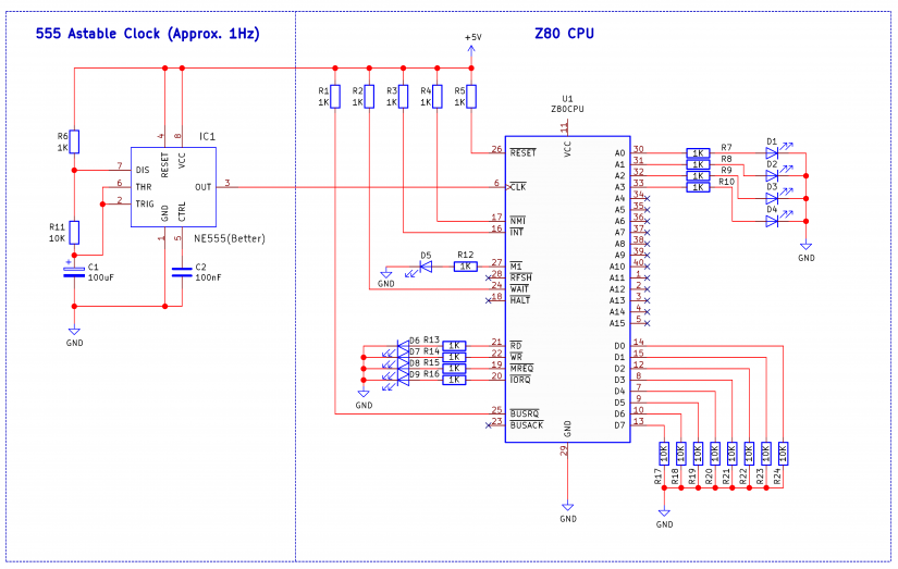 This circuit is a good tool for seeing how the Z80 works, and checking if the processor is indeed working. The first sub-circuit to the left of the schematic is a 555 astable oscillator that outputs a square wave with a frequency approximately 1Hz. This allows us to watch each cycle of the Z80 as it performs its instruction cycles. The right side of the schematic is the Z80 processor itself and you will note that some pins are pulled up to 5V, some are pulled down to 0V, and others have output LEDs. Pins that are pulled up are input control signals and it is essential that they are pulled up because the Z80 uses active-low logic. Take for example, the RESET pin, when this pin is 0V the Z80 will reset, and if this pin is 5V then the Z80 will carry on as normal.
Z80 Input Pins
- CLK – This is the Z80 clock input. Without it, the Z80 cannot function
- RESET – This will reset the processor back to address 0 as if it had just been turned on
- NMI – This is the non-maskable interrupt. When pulled low, the Z80 will perform an interrupt
- INT – This is the maskable interrupt. When pulled low, the Z80 will perform an interrupt if the internal interrupt flag is set
- WAIT – When this pin is pulled low the Z80 will sit and wait (i.e. stall). Once this pin goes back to 5V, the Z80 will resume operation
- BUSRQ – When pulled low, the Z80 will allow other devices to control the bus (address and data pins)
Some pins in the schematic are connected to LEDs, this is so we can see what those pins are doing.
Z80 Output Pins
- M1 – This pin outputs 0V when the Z80 is executing the first machine cycle
- RFSH – This is the output pin used for refresh logic, we don’t need to know about this
- HALT – This pin outputs 0V when a HALT instruction is executed
- RD – This pin outputs 0V when the Z80 is performing a read operation
- WR – This pin outputs 0V when the Z80 is performing a write operation
- MREQ – This pin outputs 0V when the Z80 wants to read from memory (RAM or ROM)
- IORQ – This pin outputs 0V when the Z80 wants to access an I/O device (keyboard, monitor etc.)
Z80 Data Pins
- A0 – A15 – These pins are the address pins and are active high. These pins select which address of memory is being accessed, or the I/O device being used
- D0 – D7 – These pins are the data pins. These will either output data from the Z80 or read it from an external memory/device
If we build this circuit and let it run, we would see that the LEDs blink in specific patterns as the Z80 continuously reads the NOP instruction (data 0x00). Why does the Z80 read NOP instructions, and how do memory read and write cycles look?
Memory Read/Write Cycles
Memory read and write cycles are the steps which the Z80 takes to get data from memory, or store it into memory. These cycles are based on how parallel memory chips work with their CS, OE, and WR signals. The image below shows a memory read and write cycle side-by-side.
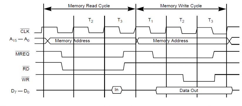 When the Z80 first starts it begins by reading the first instruction in memory at address location 0x0000. To get this instruction, the Z80 starts by setting the address pins to 0x0000, and then sets M1 to low. M1 indicates that the Z80 is at the start of a brand new instruction cycle. On the falling edge of the first clock pulse, the Z80 sets the RD pin to low to indicate that it wants to read data from the outside world, while the MREQ pin goes low to indicate that the Z80 wants to read data from memory. The next clock cycle, T2, is an extra cycle that gives external memory time to settle and produce its output. The third clock cycle sees the Z80 read the data in on the data pins, and the rising edge of the third clock cycle has the Z80 reset the RD and MREQ pins back to 5V. The data that was read will be an instruction, and the Z80 will either execute the instruction or get more data from memory to complete the instruction. Because we have connected all the data inputs to 0V, the instruction will be 0x00 which is the NOP instruction (no operation).
When the Z80 wants to write to memory, it first sets the address pins to the location it wants to write to. On the falling edge of the first clock, the MREQ pin is set to 0V to indicate that it wants to save to memory, and the data pins are set to the data that is to be saved. On the falling edge of the second clock, the Z80 sets the WR pins to 0V which causes the data on the data bus to be saved into the memory chip that has been selected. On the falling edge of the third clock cycle, the Z80 sets WR and MREQ to 5V to indicate the ending of the write cycle.
Conclusion - Dissecting the Z80
This first episode in the Z80 project series demonstrates how simple it is to get the Z80 operational. Only a few components are needed, and already the CPU is executing NOP instructions with no need for multiple power inputs, multi-phased clocks, or complex supporting hardware. The Z80 is incredibly powerful, and its architecture is great for creating multi-threaded operating systems, or even custom real-time systems. In the next episode, we will look at implementing RAM and ROM to get our Z80 to run simple programs!

Robin Mitchell is an electronic engineer who has been involved in electronics since the age of 13. After completing a BEng at the University of Warwick, Robin moved into the field of online content creation developing articles, news pieces, and projects aimed at professionals and makers alike. Currently, Robin runs a small electronics business, MitchElectronics, which produces educational kits and resources.


Leave your feedback...