
Z80 Computer Memory Explained
Previously, we looked at what the Z80 processor was, what its external control signals do, and how it loads instructions externally to execute. While all processors are different, all have the same foundations which they use with one of those foundations being memory.
Memory in a computer is an area where information can be stored for later use. Memory can be used to hold instructions for the CPU to execute as well as data for the CPU to manipulate. The Z80is a von Neumann CPU meaning that the instructions and data are stored in the same memory space (i.e. both are accessed using the same bus). Learn all about Z80 computer memory!
Parallel Memory
Before we can start to utilize memory in our simple Z80 computer, we first need to learn what parallel memory is, how it works, and the types of parallel memory in existence. Parallel memory is memory whose stored data is accessed in one single cycle. For example, an 8-bit memory chip stores 8-bit numbers, and the data bus that allows the outside world to load and save to the stored numbers can access all 8-bits at the same time in parallel. Serial memory, however, only allows for one bit of a number to be accessed at a time, and thus an 8-bit serial memory chip would require a minimum of eight cycles to access a single number.
In a memory chip, data is stored in a large table with each entry in the memory having a unique address. Each address can be accessed by using the memory chips address input pins, and the address input pins represent a binary number. The table below shows the word “HELLO!!!” stored in memory, and how each character has its own unique memory location.
| Address | Data Contents |
| 0 | H |
| 1 | E |
| 2 | L |
| 3 | L |
| 4 | O |
| 5 | ! |
| 6 | ! |
| 7 | ! |
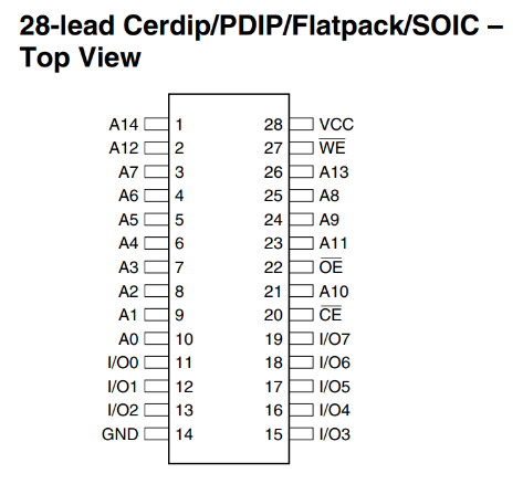
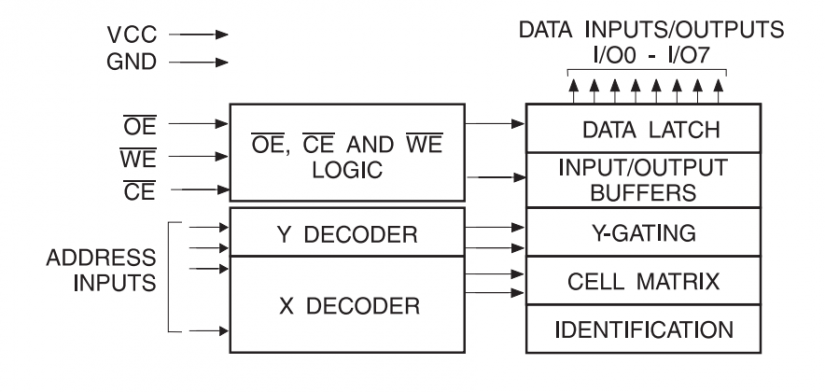
Parallel memory chips have three control signals, an address input, and a data bus.
- WE – Write Enable. When this pin goes from high to low, the number currently present on the data bus is saved to the address location equal to the address pins
- OE – Output Enable. When this pin goes from high to low, the number stored at the address location equal to the address pins is sent to the data-bus
- CS – Chip Select. If this pin is low, then the memory chip can be read and written to. If this pin is high, the memory chip is disabled and cannot be accessed
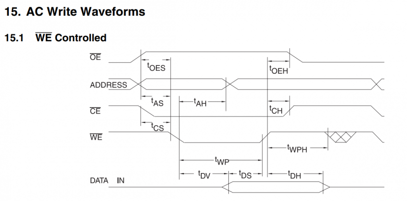
Parallel Memory – How to save data
To save data to a memory chip the following cycle needs to be done (high means 5V, low means 0V)
- Start off with the WE, OE, and CS pins as high
- Set the address location that needs to be saved to using the address pins
- Set the data pins to the data that needs to be saved
- Set CS to 0V
- Set WE to 0V <- This is where the data is saved
- Set WE to 5V <- Completed
Parallel Memory – How to read data
- To read data from a memory chip the following cycle needs to be done (high means 5V, low means 0V)
- Start off with the WE, OE, and CS pins as high
- Set the address location that needs to be loaded from using the address pins
- Set CS to 0V
- Set OE to 0V <- The data immediately appears on the data pins
- Read the data from the data bus
- Set OE to 5V <- Completed
Memory Technologies
Multiple memory technologies which all have their own advantages and disadvantages. But all memories fall into either volatile or non-volatile memory. Volatile memories are those that forget their information when they are turned off while non-volatile memories remember their stored data even when there is no power.
Volatile Memory
DRAM stands for dynamic random-access memory and is one of the cheapest memory technologies. Each bit in memory is a single transistor and capacitor whereby the capacitor stores electric charge that represents either a 1 or 0. While this memory is cheap, it quickly forgets its data even when powered meaning DRAM requires special refresh cycles. In our Z80 computer, we will completely avoid this memory as it is not the easiest to use.
SRAM stands for static RAM and is the fastest memory technology available. Each bit in this memory is an SR latch that means there are no need for refresh cycles. However, these are more expensive than DRAM but this is the memory that we will be using for our RAM.
Non-Volatile Memory
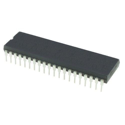
EPROM stands for Electrically programmable read only memory and remembers whatever it has been programmed with (even when there’s no power). However, these memories can only be programmed once (unless it has a glass window in which case it can be erased with UV light). This memory is archaic and will not be used.
EEPROM stands for electrically erasable programmable read only memory. This memory is like EPROM except that it can be erased using electricity. This is the memory that we will use as our ROM as it is simply to use and easy to reprogram. However, we will only read from this memory as these chips can only handle around 10,000 write cycles before they stop working.
FLASH memory is a common memory technology found in solid-state drives and USB memory sticks. This memory is somewhat complex to use as these technologies often require reads and writes that are done in blocks.
RAM vs ROM in a computer
Our computer will have two sections of memory known as ROM and RAM. The ROM section of our computer will hold program code that the computer starts to execute when it first boots. The RAM section of our computer will be used to hold variables and other data that may change during operation. However, a Z80 computer can run programs held in RAM, and a simple bootloader can preload RAM with a program before the Z80 turns on.
Since the Z80 starts executing code at address 0 when it first turns out, our ROM has to be located at address 0. The Z80 has a 16-bit address meaning that it can access a maximum of 64KB memory, and thus to keep things simple, we will divide our memory in half with the first being ROM and the second being RAM. Thus, our ROM will be 32KB with an address range between 0 and 32767 while RAM will range between 32768 to 65536. These numbers are not the nicest to use so from this point on we will use hexadecimal (0 to F). Therefore, our memory address has the following pattern:
| Memory Range | Memory |
| 0x0000-0x7FFF | ROM |
| 0x8000-0xFFFF | RAM |
Memory Management
So now we know how we want our memory to be split up, but how do we achieve this? In this case, we can use the 74139 which is a decoder chip that takes two address inputs, an enable signal, and produces four select lines. If we connect the 74139 to A15 only then the 74139 will select the ROM chip for address lower than 0x7FFF and select the RAM for address greater than 0x8000. To find out why, research the truth table for the 74139 and refer back to the Z80 memory cycle.
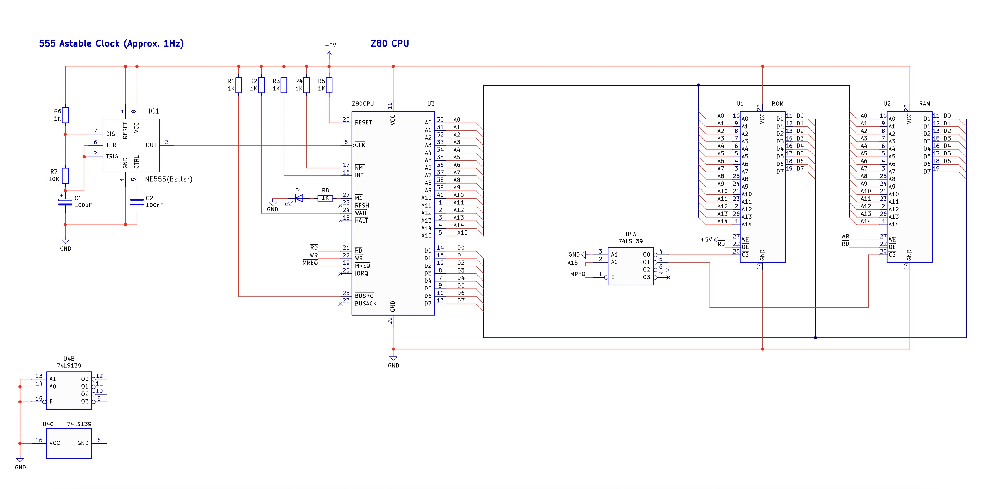
Our System
If we include the memory into our schematic we get the following layout.
Conclusion
When our system boots, the Z80 will now start to read instructions held in the ROM, and can use the RAM to store information. However, our ROM is empty and so in the next project we will learn how to make an EEPROM programmer to put information into the ROM for writing our first Z80 programs!

Robin Mitchell is an electronic engineer who has been involved in electronics since the age of 13. After completing a BEng at the University of Warwick, Robin moved into the field of online content creation developing articles, news pieces, and projects aimed at professionals and makers alike. Currently, Robin runs a small electronics business, MitchElectronics, which produces educational kits and resources.


Leave your feedback...