
What is a PCB
Chances are that you've probably seen, and have definitely used, a printed circuit board (PCB). But how much do you actually know about them? Here’s a complete guide to what circuit boards are and how they’re made!
What is a Printed Circuit Board?
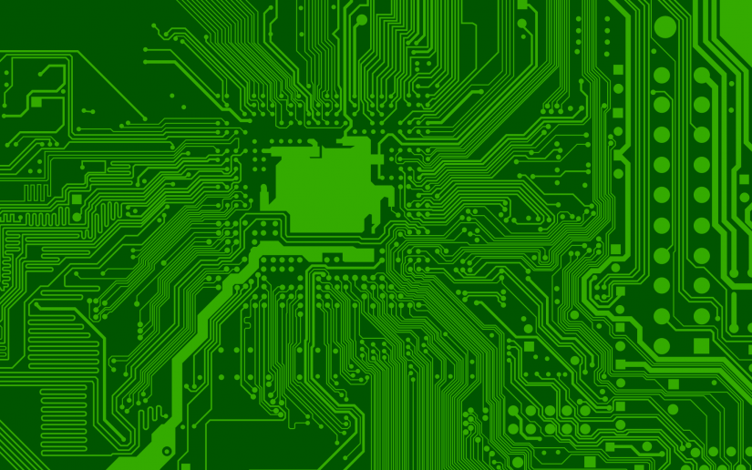
PCB stands for printed circuit board with a history that goes back to the 1940s. PCBs are the bare boards that are then populated with various electronic devices such as semiconductors, diodes, capacitors, resistors, and many other components that fulfill a specific electrical function. In addition to providing a physical foundation for these components, printed circuit boards enable electrical conductivity using pathways that allow them to communicate.
Usually, these conductive tracks are etched from copper sheets that are laminated onto a non-conductive surface. A PCB may be a relatively simple single-sided board or a more complex multi-layer circuit board.
What are PCBs Made of?
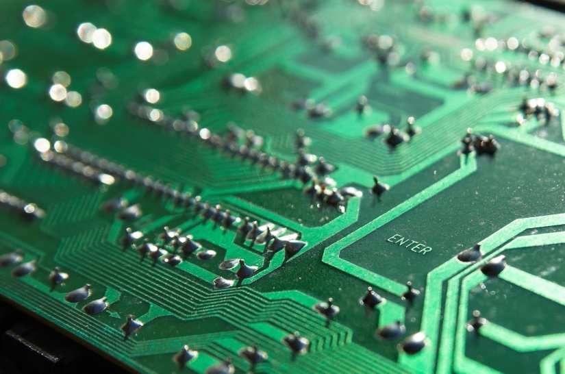
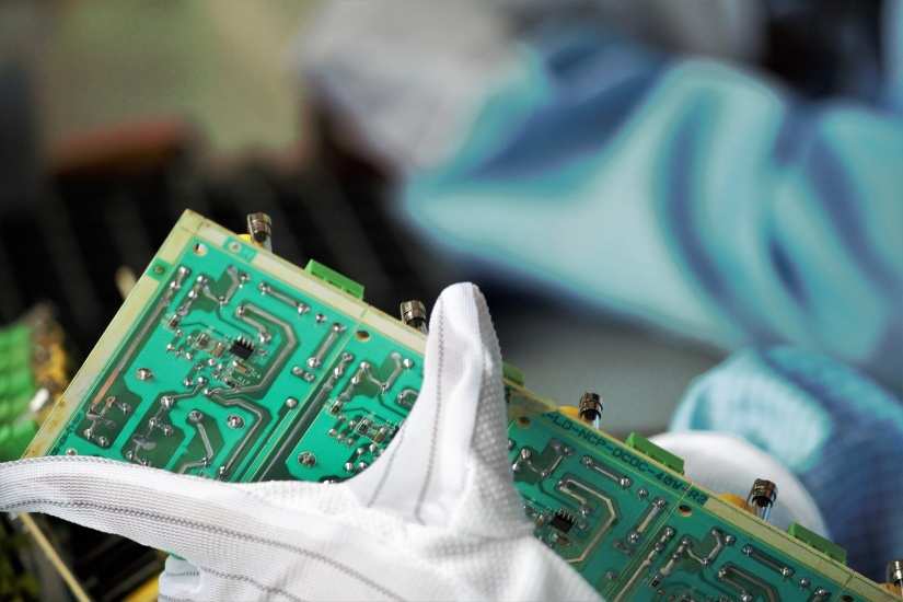
Printed circuit boards are made of several different components. Conductive strips made of copper run along the PCB and function as electrical pathways. Components like diodes, capacitors, resistors, and semiconductors are populated onto a PCB and communicate with one another through signals sent via these copper conducting strips. The electronic components are soldered onto the copper pads that are connected to the tracks with an alloy which, like copper, is an excellent conductor.
The board itself is made of a non-conductive material (for example FR-4) which can also feature silkscreen (legend) and soldermask. It's the soldermask that gives a PCB its recognizable green coloring. The soldermask insulates the copper to protect the PCB and also prevent short circuits during soldering. On top of the soldermask silkscreen is applied, with various numbers and letters printed onto the PCB to help easy identification of vital information about the board and attached components.
PCB Components
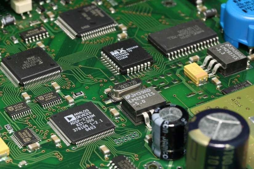
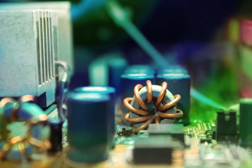
A PCB populated with its components has a similar look as a town seen from above. The components are buildings in which various functions are performed and the traces on the board are the transportation routes on which people move from building to building bringing information and goods needed by what is going on in the neighboring building. On the way over there are traffic lights, bumps, and accelerators. All like a big city, buzzing with life.
There's a battery, or another power source, that delivers energy to power the circuit (current and voltage). Transistors act as digital or analog switches that help direct electrical current traveling throughout the circuit. Resistors help regulate the electrical current traveling around the circuit and control it; the larger ones are color-coded to determine their value of resistance by sight. Meanwhile, diodes allow or block the flow of an electric current thereby dictating in which direction current can pass. Capacitors store a charge, and LEDs or light-emitting diodes light up when sufficient current passes through them.
- Power source (such as a battery): provides power to the circuit as a voltage and current source
- Transistors: controllable digital or analog switches that turn current paths ‘on’ or ‘off’, or regulate the amount of current that can pass through.
- Resistors: current flow regulation and circuit control
- Diodes: allowing flow of current only in one direction and voltage regulation
- Capacitor: electrical charge storage
- LEDs: Light up when a current passes through; current can only pass in one direction
- Conductive copper tracks: carries current and signals
- Soldermask: non-conductive insulation layer
- Silkscreen: applied on top of the soldermask with numbers and letters to provide vital information to engineers and makers
What are the Different Types of PCBs?
PCBs come in all shapes and sizes. Generally, there are three main types of PCBs: single-sided boards, double-sided boards, and multi-layer boards.
A single-sided PCB is a simple board with one layer of circuitry and a single substrate. Each component is electrically connected to one side of the board. A single-sided PCB is best for simple technological applications as all copper connections need to fit on one side.
Double-sided PCBs are extremely common and have traces and pads on both sides of the substrate connected to each other via plated through holes. A dual-sided populated board includes components attached to both sides of the printed circuit board. If a mix of surface-mount technology (SMT) and through-hole technology (THT) is used, generally the SMT will sit on both sides where the THT only sits on one side.
Designs with increased complexity require a multi-layer circuit board that has many copper layers which are separated with non-conductive FR-4 material. Since conductive and insulating layers must be paired, a multi-layered PCB usually includes an even number of layers. Often, it's four or more, and while 8 or fewer layers is the most common, some complex designs may have more than 40 layers.
Types of PCBs:
- Single-sided PCBs: All electrical components are fixed to one side of the substrate as are all the copper traces. Using through-hole technology components, this places each of them on an opposite side of the board whereas with surface mount technology components they all sit on one side.
- Double-sided boards: Copper traces and electrical components are found on both sides of the board.
- Multi-layer PCBs: Four or more layers, consisting of conductive copper layers separated by insulating substrate layers.
What Does a PCB do - Real-world Uses of PCBs
While you can probably recognize a PCB by its typical green color and copper features, as well as assembled components, what does a PCB actually do? Since printed circuit boards serve as the backbone for most electronic devices, they're some of the most common elements that you almost never see first-hand. That's because many PCBs come in many consumer electronic devices that are rarely cracked open.
Household electronics such as smartphones, tablets, smartwatches, Blu-ray players, game consoles, TVs, microwaves, and refrigerators all rely on PCBs. One of the best and most prominent examples of a PCB is a computer motherboard.
Outside of consumer electronics, PCBs are often deployed in industrial as well as medical devices. Power supplies, power inverters, and manufacturing devices to control temperature or pressure all use PCBs. In the medical realm, X-ray and ultrasound machines, medical monitoring devices for heart rate or blood pressure, and even microscopes all contain PCBs. The automotive industry takes advantage of printed circuit boards for applications such as GPS navigation systems or in-dash infotainment centers that run Android Auto or Apple Car Play.
Where are PCBs used in the real world:
- Consumer electronics: Smartphones/tablets, smartwatches, Blu-ray players, TVs, computers, etc.
- Industrial electronics: Power supplies, power inverters, temperature control manufacturing devices, pressure control devices, etc.
- Automotive industry: GPS navigation systems, infotainment systems, etc.
- Medical applications: X-ray machine, ultrasound machine, heart rate monitor, blood pressure monitor, microscopes, etc.
What is Involved in PCB Design and Manufacturing - How are PCBs Made?
Making of a 4-layer PCB by Eurocircuits from Eurocircuits on Vimeo.
PCB design is a multi-step process. First, a printed circuit board schematic must be created. With the help of modern technologies, such as computer-aided design (CAD), a PCB may be mocked up using CAD programs. Since many CAD applications use proprietary file types, the PCB manufacturing industry developed a standardized file format, the Gerber format. Various PCB-specific features such as the ability to set the copper tracking layers, component notations, and soldermasks come standard in Gerber files. With CAD PCB layouts, it's possible to check manufacturing specifications such as the space between conductive signal traces, hole size, and more aspects of PCB design. While a lot of that is done automatically by software, manual checks may also be performed.
PCB Image Transfer - Phototool Preparation
After a PCB is designed and all checks pass, the circuit board fabrication process begins. Usually, this involves imaging the PCB. Most often, laser photoplotters in a darkroom are used to create films. A photoplotter transfers data about a board into a pixel image which is then etched onto film by a laser. The film is then developed and prepared for the PCB fabrication process. There's one phototool, or a film, for each copper layer. So a single-layer PCB will have one phototool, while a six-layer PCB for example will feature six films for the copper.
Multilayer PCB Inner Layer Imaging
Once the fabrication and phototool preparation process is complete, the inner layers of a multilayer PCB must be created. During inner layer imaging, an epoxy resin and glass-fibre core laminate is used. The copper is first cleaned, then coated with a photosensitive film layer. An exposure unit bed using registration pins corresponding to the holes in the phototools is utilized, with each layer's phototool layer image loaded onto the pins which make sure that all are properly aligned. Ultraviolet (UV) lamps in the printer then harden the photoresist, or photosensitive film, which defines the copper pattern on the PCB. All operations happen in a room with yellow lighting to account for the photoresist's sensitivity to UV light.
Today photoplotters and exposure units are replaced by direct imaging machines exposing the image with laser diodes directly onto a photosensitive layer which is applied over each copper layer.
Now, the photosensitive film must pass a developer unit to fix the image and to remove any unhardened resist, while the entire panel is pressure washed and then dried. This leaves the copper pattern completely covered by a hardened resist.
Etching the Inner Layers
Unnecessary copper needs to be removed which is accomplished using an alkaline solution that etches away unwanted exposed copper from the inner layer of the PCB. After that, the photoresist protecting the copper image is removed.
Inner Layer PCB Production Registration and Inspection
With the multilayer PCB core finished, it's time to punch registration holes. These are used for aligning the inner and outer layers of the PCB as a whole. The core is loaded into an optical punch that aligns with the registration targets within the copper pattern. An automatic optical inspection system will then scan the board and compare the physical object with a digitally-rendered image to identify any errors.
Bonding and Lay-up
After punching registration holes, the outer layers of the multilayer PCB are bonded and pressed. A bonding press heats up press plates which apply pressure that bonds the different layers in the PCB together. The heat melts and cures the epoxy resin in the prepreg while the pressure bonds the PCB together. Once the desired heat and pressure levels are reached, a cool-down initiates.
Drilling the Holes
With all PCB layers bonded, holes need to be drilled. This requires an X-ray drill to pinpoint the desired targets in the copper of inner PCB layers. Then, a panel of exit material is placed on the drill bed which prevents the drill from ripping the copper foil when it penetrates the PCB, after which PCB panels and a sheet of aluminum entry foil are loaded up. Now, the drilling machine, powered by air-driven spindles capable of rotating at up to 200,000 revolutions per minute, creates each hole. When finished, the exit and entry materials may be thrown away.
Plating the PCB
With the bonding and hole drilling completed, the PCB must be plated. Initially, a chemical deposit of a thin copper layer is applied to the PCB surface and hole walls using an electroless copper. These days it is more common and more environment friendly to apply a layer of black oxide (a carbon solution) instead of chemical copper.
After that's finished, the outer layers of the PCB are imaged in a clean-room to ensure the panel surface is dust free. Similarly to the inner layers, a photosensitive film is laminated onto the panel.
A printer with pins matching the holes in the panel and phototools is used with the first film loaded onto the pins, followed by the laminated panel, and lastly the second film. The pins keep the bottom and top layers aligned. UV lamps harden a photoresist.
Today photoplotters and exposure units are replaced by direct imaging machines exposing the image with laser diodes directly onto a photosensitive layer which is applied over each copper layer.
The Mylar film that protected the photoresist gets removed, and the photosensitive film must now pass a developer unit to fix the image and to remove any unhardened resist, while the entire panel is pressure washed and then dried. This leaves the copper pattern and the holes that need plating completely free of hardened resist. The boards can now be plated with copper.
Post-processing - Soldermask, Silkscreen, Electrical Test, and More
A soldermask is usually applied at this stage. An epoxy ink soldermask gets printed onto both sides of the PCB, its purpose to protect the copper surface of the board. Today, two processes are used to apply the soldermask. Soldermask has a tremendous influence on the further assembling of the boards with components. That is the reason for constant improvements on the soldermask material and the ways of applying the soldermask on the boards.
Since the soldermask doesn't cover the copper component pads or holes, a solderable finish is applied to the copper components in the form of an electroless gold coating over nickel or some other finishers.
Plated gold edge connectors may be necessary for a PCB. If a printed circuit board is to be frequently inserted into a connector, plated gold edge connectors are recommended. Once protective tape covers board connectors, the PCB is mounted on a panel and dipped into an electroplating bath. While electroless gold is great for soldering, its durability can't handle frequent wear and tear. As such, gold-plated edge connectors provide better durability.
The majority of PCBs feature silkscreen which serves as a sort of road map or legend to help identify onboard components. A silkscreen is applied using a digital ink-jet printer to spray ink droplets onto the board and thus create a physical silkscreen. Once the silkscreen is sprayed on, it must be cured and baked.
An electrical test needs to be performed to ensure that all of the PCB components are properly connected. Because of the design of a printed circuit board, a current is only supposed to flow in one direction. Assuming a PCB passes its electrical test, the board must be cut out of the production panel using a milling machine or router. But there's still one more step in PCB production: final inspection for quality control where inspectors check over a PCB and make sure that a board is free from physical defects. If everything checks out, the PCB is then ready to be shipped out!
PCB design and manufacturing process:
- Printed circuit board design, typically in CAD software (Output Gerber Files)
- Checking of PCB design elements (i.e. space between conductive tracks, hole sizes, etc.)
- PCB fabrication begins with PCB imaging
- Inner layers printed
- Etching of inner layers
- Automatic optical inspection
- Bond and lay-up
- PCB drilling
- Outer layer imaging
- Plating
- Outer layer etching
- Soldermask application
- RoHS-compliance surfacing
- Plated-gold edge connections
- Curing and silk-screening
- Electrical testing
- Profiling
- Final inspection
What is a PCB - A Primer on PCBs
PCBs are some of the most common electronic devices that you may never see. While they're crucial to powering many household objects such as computers, TVs, game consoles, and microwaves in addition to many medical, automotive, and industrial electronics, printed circuit boards are mostly tucked away from sight. Still, they're easily recognizable from their striking green coloring, a result of a PCB's soldermask, and the copper traces adorning the board like roads.
Coming in a variety of shapes and sizes, PCBs may be simple, single-layer boards or complicated multi-layer devices. PCB manufacturing is a multi-step process that begins with a CAD mock-up and wraps up with electrical testing, routing, then quality control testing. You can think of a PCB as the heart that powers your favorite electrical devices, sitting unseen behind layers of plastic and other electronic components, but pumping the lifeblood of that device.

Moe Long is an editor, writer, and tech buff with a particular appreciation for Linux, Raspberry Pis, and retro gaming. Writing online since 2013, Moe has bylines at MakeUseOf, TechBeacon, DZone, SmartHomeBeginner, DEV.to, DVD Netflix, and Electropages. You can read his writings on film and pop culture at Cup of Moe, check out his tech reviews, guides, and tutorials at Tech Up Your Life, and hear his thoughts on movies on the Celluloid Fiends podcast. Aside from writing and editing, Moe has an online course, the Beginner's Guide to Affiliate Blogging From Scratch. When he's not hammering away at his keyboard, he enjoys running, reading, watching cinema, listening to vinyl, and playing with his dog Sebastian.


Leave your feedback...