

My First Real Pcb Artwork ?

Made by vin-vout-io / 3D Printing / Art / Lights
About the project
Turning circuit boards into storytelling canvases—where every trace, layer, and silkscreen becomes part of the art
Project info
Difficulty: Moderate
Platforms: Texas Instruments, KiCad, OSH Park, PCBWay
Estimated time: 1 hour
License: GNU General Public License, version 3 or later (GPL3+)
Items used in this project
Hardware components

Story
Hey everyone!I’m excited to share my latest PCB art project, where I’ve combined electronics and design into a unique piece of functional art. Let’s dive in!
If you have been following me you'll probably know that I am into pcb artworks, but eventhough I have done some works but none of them where a proper pcbart work I would say because none of them actually utilised different layers available to a pcb, because I didnt knew how to use the layers properly inorder to create different shades to the pcb board but in this one, I would say is a proper pcb artwork
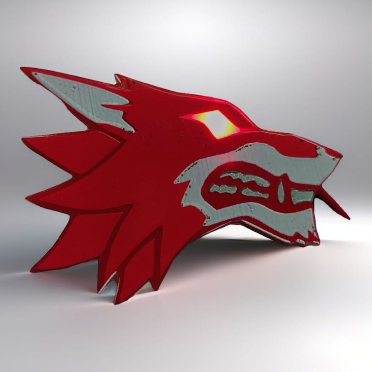
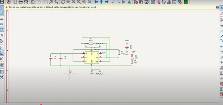
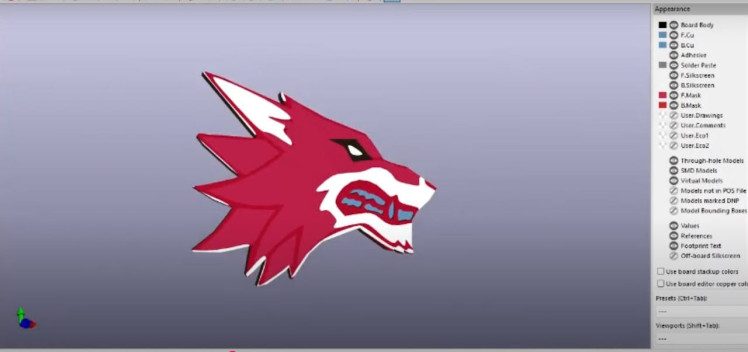
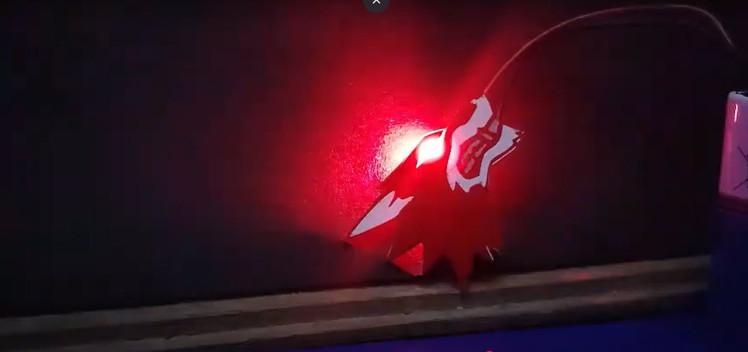
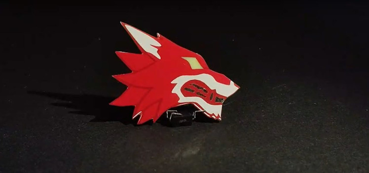
For this project, I designed those coyote-shaped pcb artwork, the circuit is a simple 555 timer circuit which operates in the astable mode
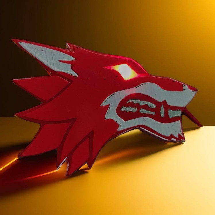
This one is different. This Coyotee-themed PCB is what I consider my first real PCB art piece. It’s the first time I truly used the layers — copper, solder mask, and silkscreen — to create depth, contrast, and shading, just like an actual canva
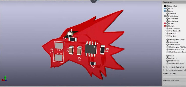
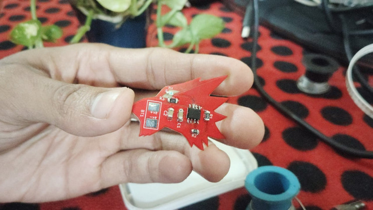
The Design and Fabrication ProcessI designed this PCB using Kicad. One of the fun parts was arranging the traces and silkscreen to form the final artwork. Because arranging these layers in an order gives you different shades to your pcb.
1 / 6
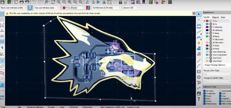
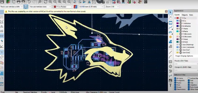
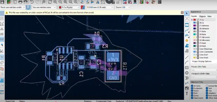
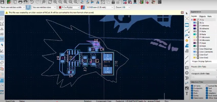
The stacked layers create a beautiful color palette which starts with the darkest layer, the masked fiberglass. The layers get lighter with the masked copper and exposed tinned copper layers. In order to create artwork from PCBs I will take advantage.
1 / 2
- Sillscreen → F.SilkS
- Copper → F.Cu

- Bare FR4 → F.Mask (inverted)
1 / 2
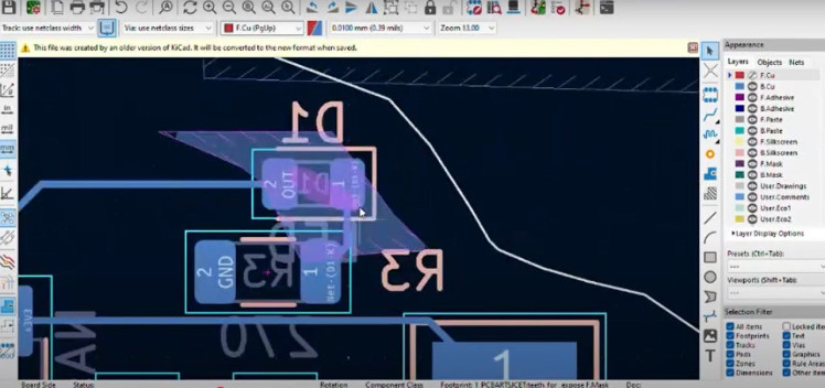
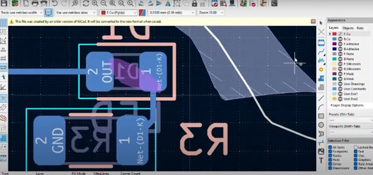
- Teeth → F.Mask, F.Cu

- Dark red → no need as without copper area and soldermask will appear as dark red
Outlines
Outlines
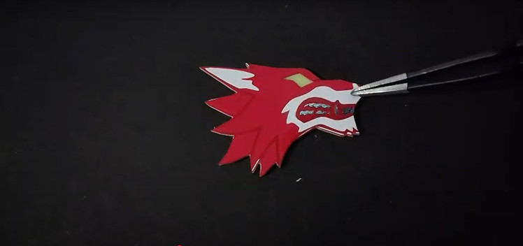
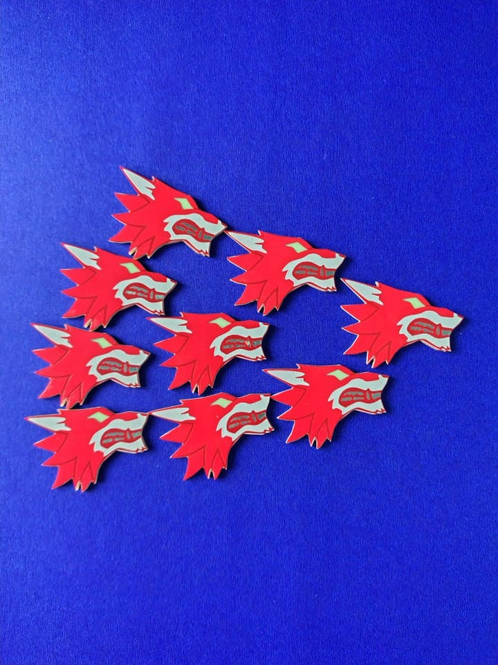
Once the design was ready, I sent it for fabrication.
PCB Fabrication -- PCBWayOnce our design is ready, PCBWay takes the reins, ensuring our PCBs are fabricated flawlessly. When we receive our PCBs, we'll move on to the assembly stage. A huge shoutout to PCBWay for making this process smooth and enjoyable! https://www.pcbway.com/

They provide high-quality printed circuit boards (PCBs) at unbeatable prices. Look no further than PCBWay, your one-stop solution for all your PCB needs!
Why Choose PCBWay?
Quality: They take quality seriously. The PCBs I got are of excellent quality and they are really gorgeous.
1 / 4


You can get 10 PCBs just for 5$

Quick Turnaround: Time is of the essence in the tech world. PCBWay offers blazing-fast manufacturing and delivery times, so you can bring your ideas to fruition faster than ever before.

Easy Online Ordering: Their user-friendly online platform makes ordering PCBs a breeze. Simply upload your design files, customize your order, and that's it.
Assembly Services: PCBWay offers PCB assembly services to save you time and effort. From components sourcing to assembly and testing, PCBWay has your assembly needs covered.

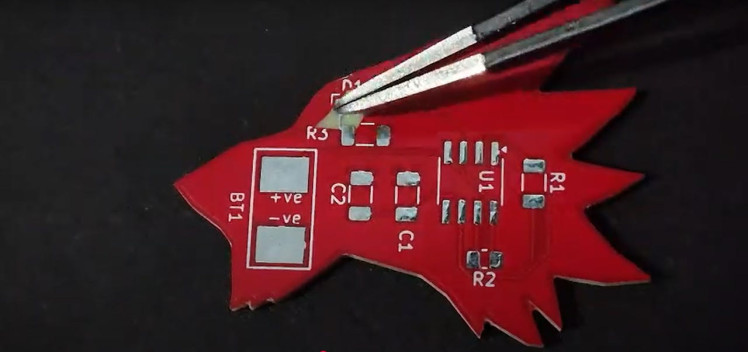
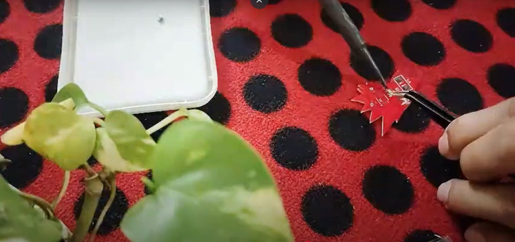
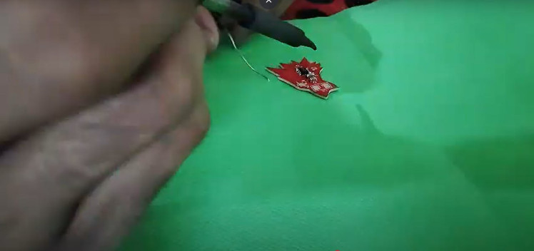
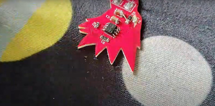
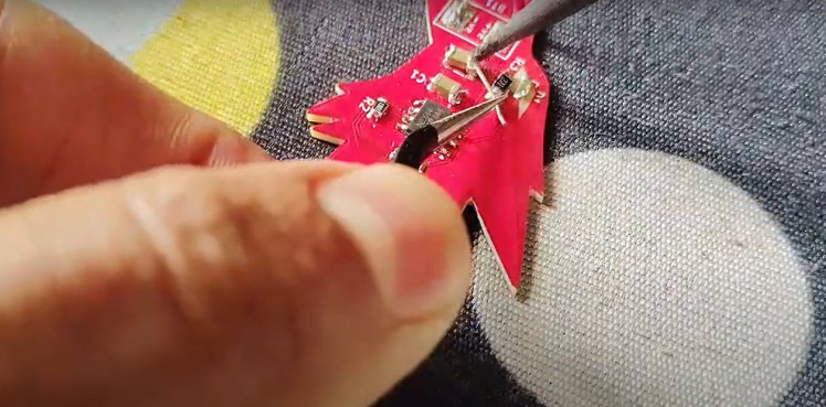
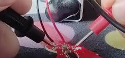
Now comes the exciting part—bringing this PCB to life! I carefully soldered the components to make it both artistic and functional.
1 / 3
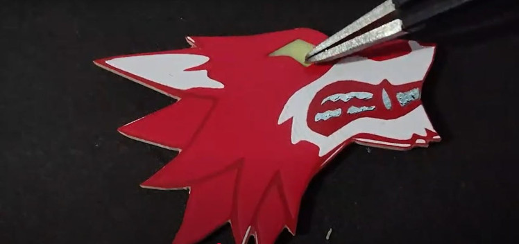
I have made the smd led soldered upside down purposefully to the board so that it can shine through the fr4 material
1 / 2
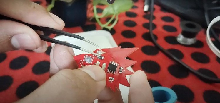
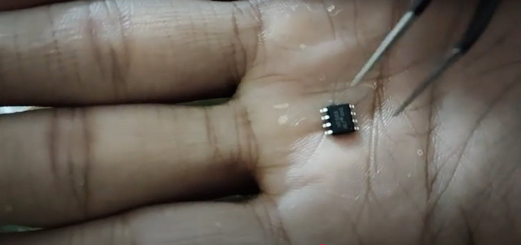
This was my first time making a board completely using smd component
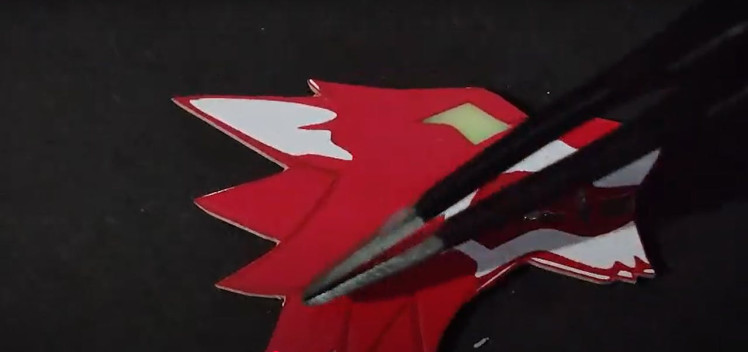
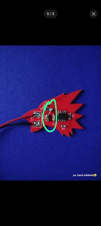
I have made a design error, I have been trying to figure out the what the problem was, I actually spend a coupleof days, and while I was checking continuity on the board
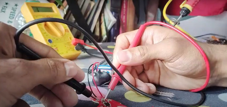
only in one part there was no continuity, between this capacitor and the led, as I looked into it I found that the copper pour for the gnd wasnt complete there(i used copper pour for gnd connection).
This happened because the copper traces the way I arranged the components actually isolated that area from getting the copper pour, I understood my mistake, you learn from mistake.
1 / 3
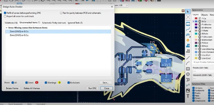
The warning would have shown in kicad but accidentally I think I ignored it because there will be showing other errors related to the silkscreen, edges etc.. would be always showing when designing our artworks as this isnt conventional so I accidentally ignored it. Any way I studied a lesson the hard way
1 / 2

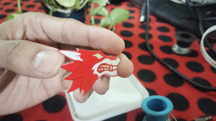
I think it turned out pretty cool.
1 / 3

I’m always experimenting with new PCB designs, and I’d love to hear your thoughts on this on
Schematics, diagrams and documents
Credits
Related products


Leave your feedback...