
World's Slimmest Neopixel Led Matrix

Made by ElectroPoint / Displays / Lights / IoT
About the project
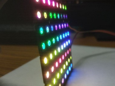
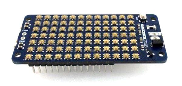
This is a 8x8 WS2812b NeoPixel LED matrix that is completely flat surface and has the same 1.6mm height as a normal PCB
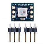
Items used in this project

Story
I always have this idea of what would have happened if we can put the components inside the pcb? Let's find out!
This is the world's slimmest addressable RGB led matrix that can be made with 5050 WS2812b neopixel LEDs. why? Because on this PCB the LEDs are not actually on top of the PCB, rather it's inside the PCB.
Luckily the height of the LEDs are the same 1.6mm, as most of the commonly used PCB thickness. That makes it possible to have a completely flat surface as well. I conduct this experiment to see how far we can push the limits of modern design tools and techniques.
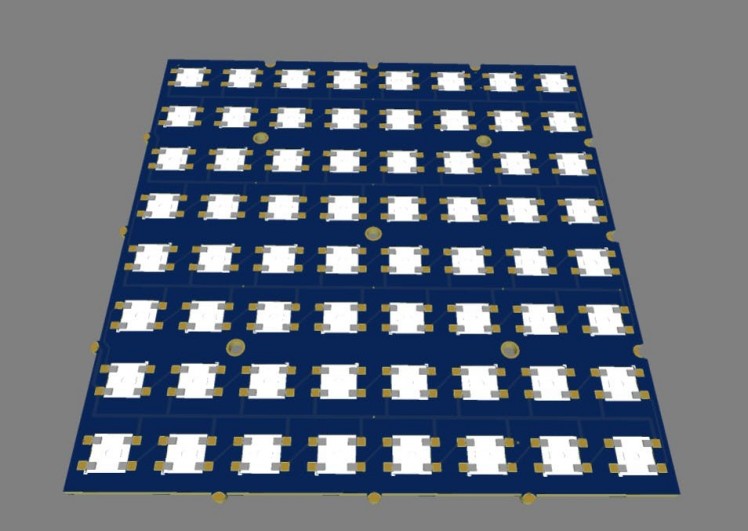
I start off by designing the board in EasyEDA. As there are no premade footprints available, I had to make my own. I did this by modifying a regular footprint. I first make the pads square and move them outside of the PCB. Then I made a cutout in the middle, slidely smaller than the size of the LED. So that it can fit tightly inside.
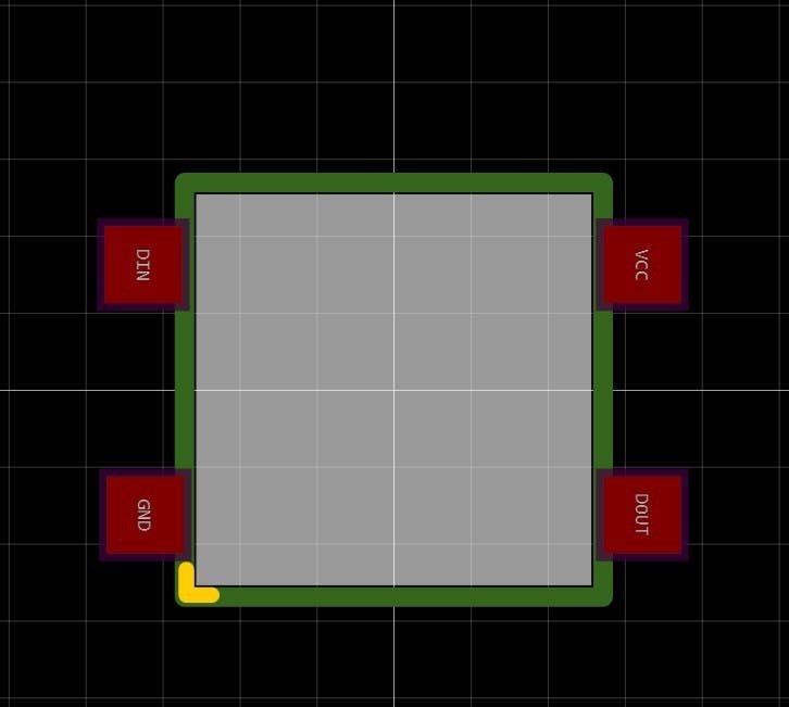
I have also added a marking to indicate the ground pad. And our footprint is ready. Then I open a new PCB and import 64 leds and arrange them in 8x8 matrix format.
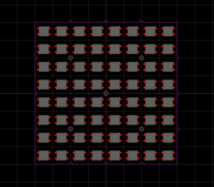
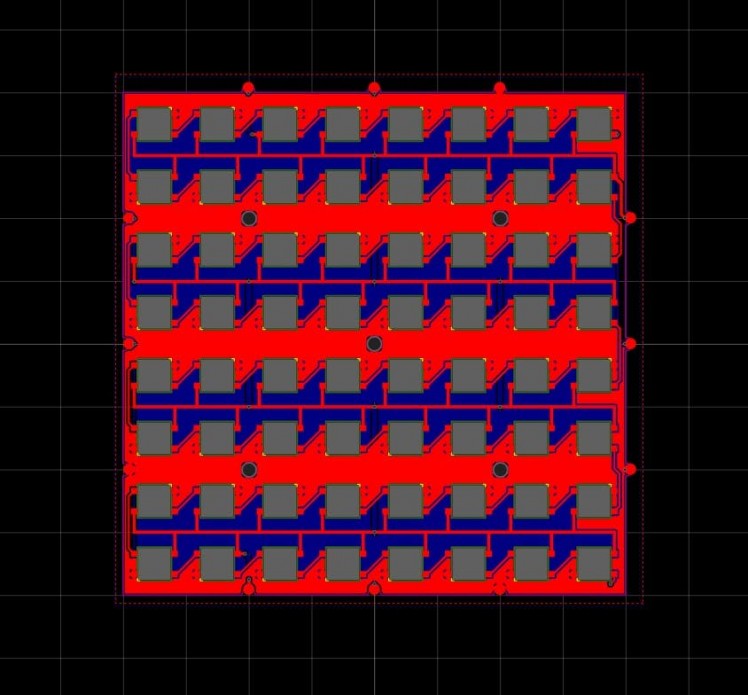
I then rotate alternative rows to be able to connect them like a chain. Next I place the nets manually followed by complete routing. Finally I added a border outline and some tabs to join them with one another and our design is complete.
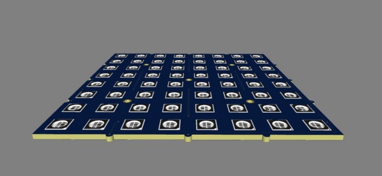
Then I head over to PCBway’s website to manufacture the PCBs. you can get the same PCBs by following this link The assembly is a tricky part. You need to push the leds from backwards in the PCB. while keeping the rotation in mind. The marking on the PCB will help you to determine the GND pad. Then I solder them one by one. It’s not that hard to do and our PCB is ready for testing.
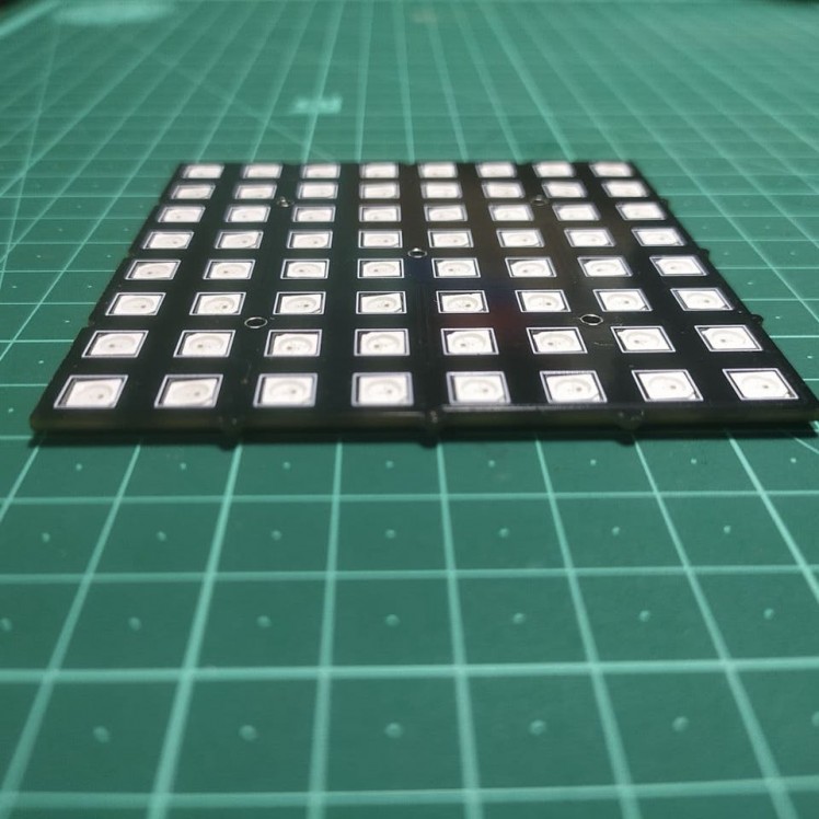
I have used Examples from the fastLED library. Which seems to work just fine. So this weird concept actually worked.
Schematics, diagrams and documents
Code
Credits
Related products


Leave your feedback...