
Hacking Qualcomm (Quick Charge) QC 2.0/3.0 With ATtiny85

Made by electrouser805 / Home Automation
About the project
Get not only 5 volts but also 9, 12 volts (18 Watts max) out of any QC-compatible charger/power bank for supplying power hungry projects.
Project info
Difficulty: Moderate
Platforms: Arduino, Microchip, SparkFun
Estimated time: 1 hour
License: GNU Lesser General Public License version 3 or later (LGPL3+)
Items used in this project
Hardware components


View all

Story
Introduction
Many USB powered consumer electronic devices have built in Qualcomm QC (Quick Charge) solution for rapid charging at different voltages rather than the usual 5.0 volts. This enables the opportunity to use QC compatible Power Banks for projects require more power or higher voltages like 9/12 volts.
The purpose of this project is to develop a device that can hack the QC protocol and allow hobbyists, developer, engineers to use their power banks for more voltage/power for their next power hungry project.
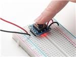
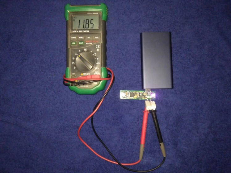 1 / 3 • 12 Volts Output from QC 2.0 Supported Power Bank
Above images show 5, 9, 12 Volts output from a QC 2.0 compatible power back powering 10 Ohms 5 Watt resistor.
Developing the Hack * Device
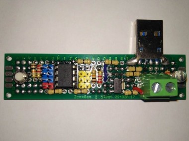
The whole device has two active components - the LM1117 3.3V voltage regulator and the ATtiny85 MCU to control. All other parts are resistors, push switch, connectors, jumpers, headers, terminal, protoboard etc.
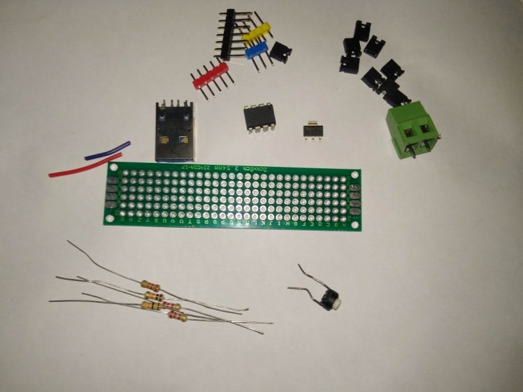 Components
To build the device, first components are places in a neat layout, then soldered. Some 0 ohms short links are used to interconnect different parts.
There are jumper to disable onborad circuit and enable programming. Since, programming line (SPI - MOSI, MISO, SCK) also acts as GPIO during device operation.
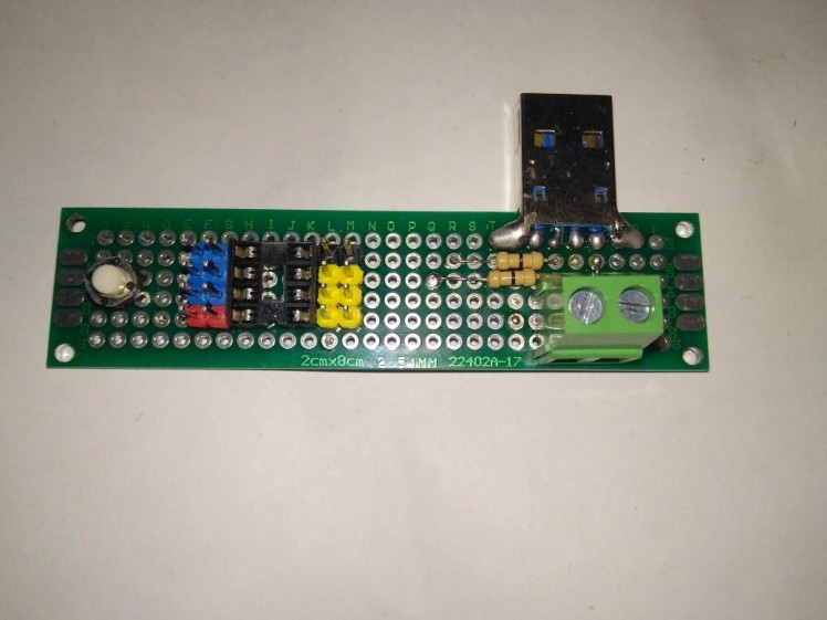 1 / 3 • Connectors, Headers, Socket, Switch placement
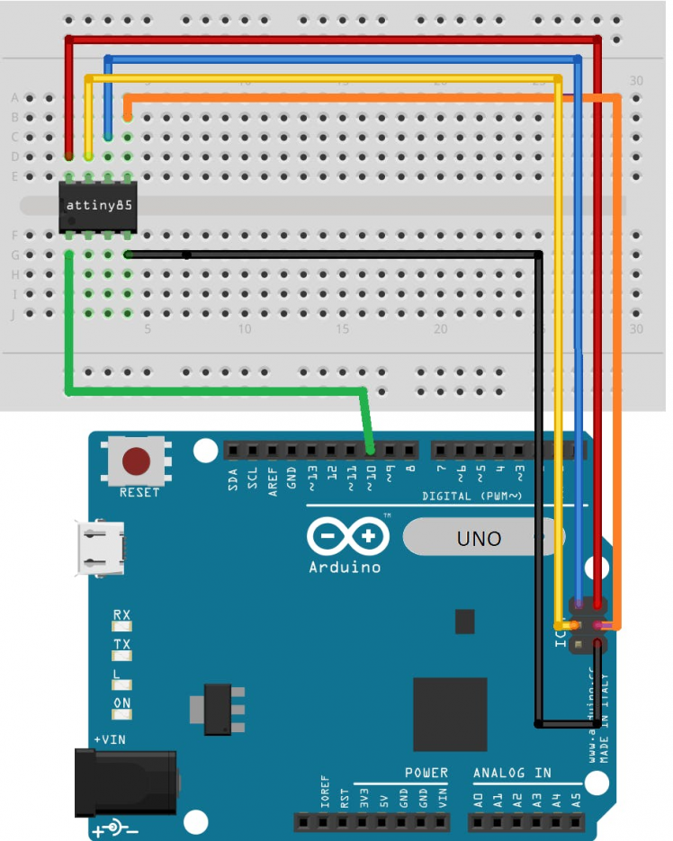
Programming ATtiny85 with ISP
Before programming the ATtiny85, it is removed from IC Base and placed on a breadboard. To program ATtiny85, an Arduino UNO board is converted to ISP programmer by uploading the " ArduinoISP" from File > Example > ArduinoISP sketch. This sketch is available in Arduino IDE.
Programming ATtiny85 requires following steps:
- Installing ATtiny support for Arduino IDE ( thanks to David A. Mellis )
- Burning Bootloader for ATtiny85 using Arduino UNO as ISP
- Developing and Uploading Code using Arduino UNO as ISP
Following circuit is prepared to program the ATtiny85:
 1 / 2 • Burning Bootloader and Uploading code using Arduino Uno as ISP
ISP = in system programmer
Alternatively, the ATtiny85 can be programmed keeping on the device by removing all the jumpers around it.
Device Operation
To use the device, first it needs to be connected to a QC compatible Power Bank (or Charger). By default the voltage of the QC Power Bank's USB will be 5.0 volts.
All the jumpers must be connected after uploading the code, so MCU can communicate over D+/- to QC source.
The LM1117 3.3 V regulator will power up and feed power to ATtiny85. This MCU will start executing the code. 4 I/O pins of ATtiny85 are connected to the voltage divider resistors which will be used as Output High and Low. Another I/O pin is connected to a switch that will initialize as input Pull Up. This switch takes user input to change the voltage of QC source.
Now, before going into details, it is important to know how the Output will change. There are at least 4 lines/wires common to every kind of USB ( USB A, B, C, 1.1, 2.0, 3.0+).
These are :-
- VBUS (Vcc +5V by default)
- D +
- D -
- Ground
In ordinary Charger/Power Bank VBUS is fixed, because of that power delivery is limited by current which may 500 mA, 1 A, 2 A yields 2.5 Watts, 5 Watts and 10 Watts respectively.
But in QC power source devices, there is an internal boost converter which can pump up the voltage depending on the power receiving device's (PD) request !!!
QC 2.0 ( also 3.0 ) utilizes D+ and D- of USB to communicate with PD. PD sends voltage signals on D+ and D- and QC charger will deliver power accordingly by changing VBUS voltage. According to this CHY Datasheet, here is a table explaining what signal pair on D+/D- from PD will make the QC to deliver what voltage output:
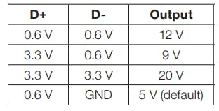 D+/D- Signal Table
QC 2.0 support initiates when voltage on D+ and D- are same as the values on 4th row of this table and stays at least 1.25 seconds. If D+ becomes 0.0 volts (below 0.325 Volts actually) QC support will stop and Output will be 5.0 volts. By setting voltages according to this table, output on VBUS can be changed.
Here, ATtiny85's 4 Output are connected to 2 voltage divider network consist of two 10k and two 2.2k resistors to generate these voltage signals for D+/D- lines.
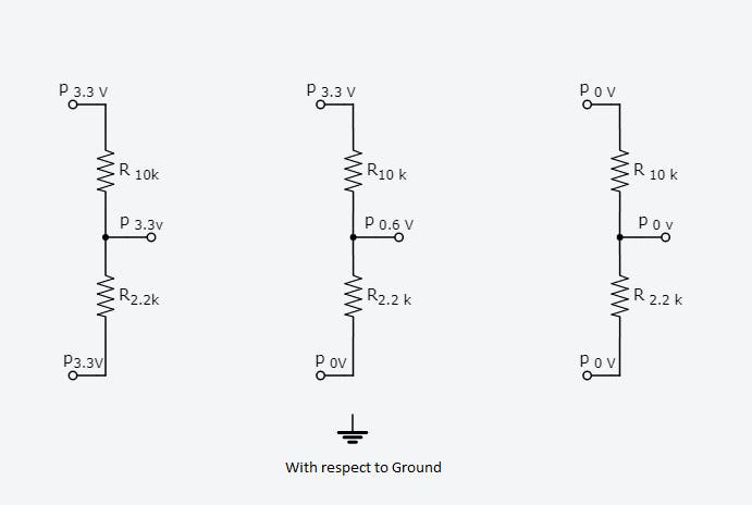 Signal Generation
For example, to generate 3.3 V on D+, both top and bottom resistors which are connected to two ATtiny85 Output pins PB3 and PB4, both will be made High from code.
Similarly, to generate 0.6 V on D-, both top and bottom resistors which are connected to other two ATtiny85 Output pins (PB1 and PB3) will be made High and Low respectively.
This way QC 2.0 charger/power bank receives voltage change request and changes accordingly. The Push Switch is configured as Input PULLUP, while not pressed, it is read HIGH by the MCU and code executions holds up in while loop preventing any change of set voltage. When user presses the Push Switch, while loop breaks and the next voltage is set. Then again, code execution enters the next while loop to hold up current VBUS voltage.
There is a LED that glows dim (5V), mild (9V) and bright (12V) to give visual representation of the output voltage to the user.
Possible Applications
- Driving 12V LED Stripes
- Powering RF transmitters/receivers for longer range
- Driving 12V Relays, Motors etc
- Get any voltage between 1.25 to 10 volts using a LM317 or LM2596
- 9V IR remote drive
- Robotic Car Power
- Laptop Charging with 20V
- Any system up to 18 Watts like WiFI, LTE, S2E devices for IoT application
- Backup power for remote systems
- Most LCD, LED Monitors, Printers, Scanners
- Low Power portable PC
Support for other QC Classes
Since QC 2.0 Class B, QC 3.0 and QC 4.0 are backward compatible with QC 2.0 Class A, therefore this device might work with all latest chargers and power banks. But voltage options will be 5.0, 9.0 and 12.0 volts. If other output voltages are needed please read CHY 100, 101, 103 datasheets and modify the code accordingly.
Warning!
- High Quality QC Power Bank or Charger with Short Circuit Protection must be used, external Loads Must Not Exceed 18 Watts. This can be ensured by Checking Power Rating Label on Load devices.
- Outputting 20 Volts Must be Avoided since 1117 3v3 regulator can Handle Maximum 15 Volts, this should be avoided from the MCU Code by Never allowing D+ and D- line having 3.3 Volts At The Same Time.
- In case 20 Volts output is required (supported by QC 2.0 Class B and QC 3.0, QC 4.0) , a voltage regulator (LM317 configured for 3.3 V) that can handle more than 20 Volts must be used. Otherwise both Regulator and MCU will be Destroyed !!!!
- Attention Should be Paid to the Output Voltage Polarity, +ve indicated by RED and -ve indicated by BLUE tiny wires next to Output Terminal.
- Loose connection at USB Male-Female coupling must be Avoided or Heat will be generated as a consequence of Contact Resistance and Power Efficiency Will Drop.
- During ISP Programming All Jumpers Must be Removed to Isolate MOSI, MISO, SCK, VCC, GND, RESET Pins from rest of the circuits on the board to Avoid Interference with Programming.
- Code modification Must Not be Done without Clearly Understanding QC Charging Protocol, This Design is Mainly Intended for QC 2.0 (Class A) Power Sources but can be partially used for Higher QC Standards
- Hack Might Not Work with some QC Chargers/Power Banks
- GPIO Switching Must be done in Proper Sequence to Avoid Termination of High Voltage Mode
Note: It is Advised not to Replicate this Project if Above Points are not Understood by someone, otherwise Risk of Fire Hazard or Loss of Equipment might occur!
It is possible to change the voltages manually without using any microcontroller. Just 4 jumper wires are required for mimicking the conditions of D+/D- table by connecting to Vcc (3.3V) and Gnd (0V) to the resistors in proper sequence. Because using mcu may be a overkill for such simple transitions after all.
References
Schematics, diagrams and documents
Code
Credits
Related products


Leave your feedback...