
Eurocircuits Pcb Design Competition Entry: Vidor Expansion
About the project
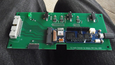
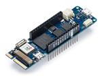
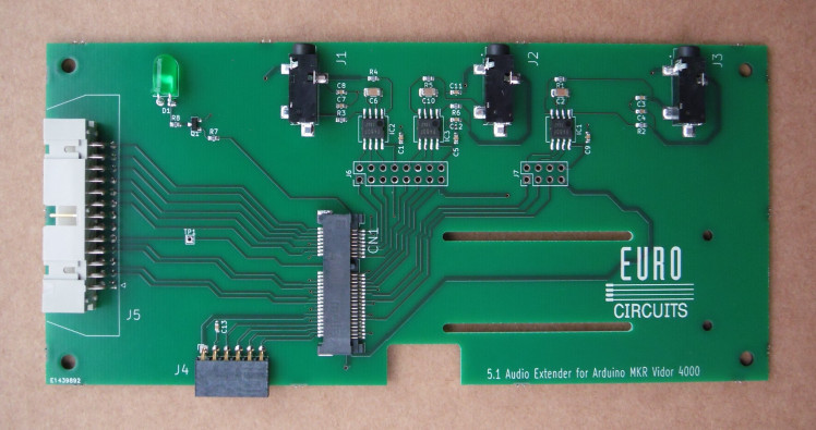
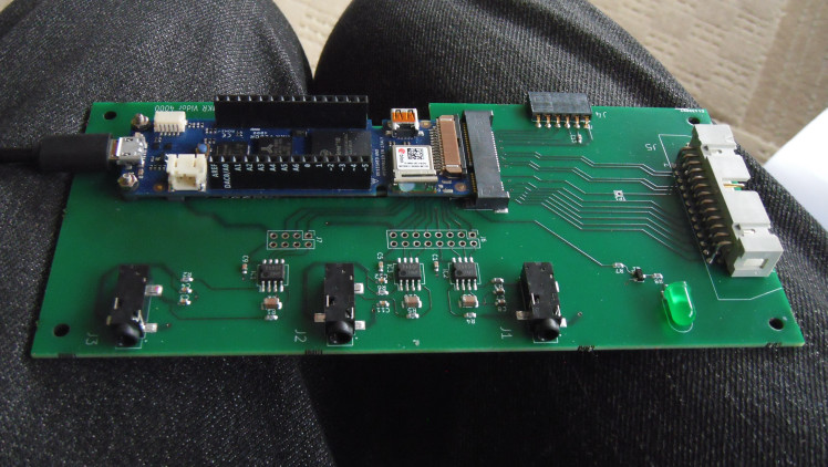
This board is used to get access to the FPGA I/O from the PCI-e edge connector on the Arduino Vidor 4000 board. Some of these signals are fed into three stereo 16-bit DACs to give 5.1 or 6 channels of audio. This board plus a Vidor 4000 will make an extremely versatile electronic musical. instrument.
Project info
Difficulty: Easy
Platforms: Arduino
Estimated time: 1 hour
License: GNU General Public License, version 3 or later (GPL3+)
Items used in this project
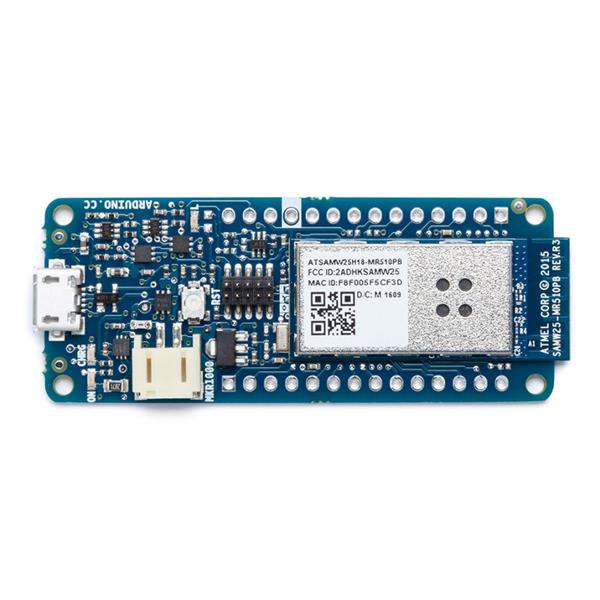
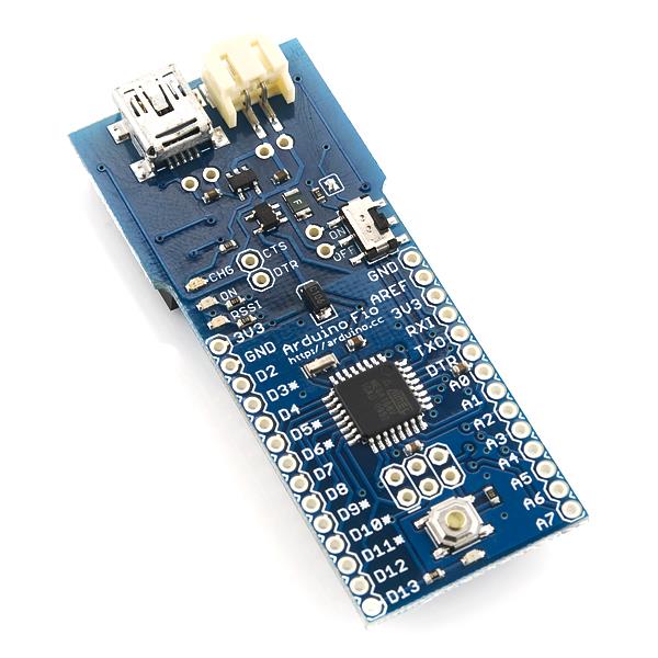
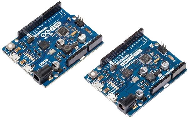
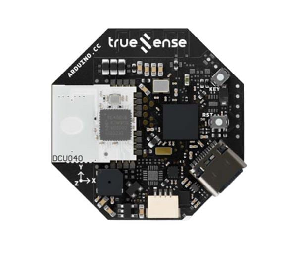
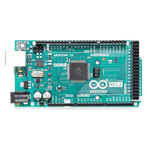
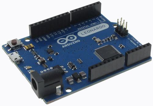
Hardware components
Software apps and online services

Story
 Project:
The idea is to build a musical instrument e.g. an electronic organ, using an Arduino Vidor 4000 and this PCB, called 5.1 Audio Extender for Arduino Vidor 4000.
My PCB:
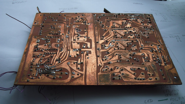
This PCB was designed using kicad 5.1.10. The kicad design files were uploaded to Eurocircuits' website for subsequent PCB manufacture and assembly.
The process checked component footprints against the tracking and flagged an inconsistency with the NPN transistor. To save time and effort, I modified the existing PCI-E connector footprint to fit the larger size of the Vidor 4000.
Note that the bottom copper layer is a 0V ground plane. I always try to do this technique because it reduces noise levels and allows impedance matched tracks at the higher frequencies. It is also quicker and 'greener' if less copper has to be removed.
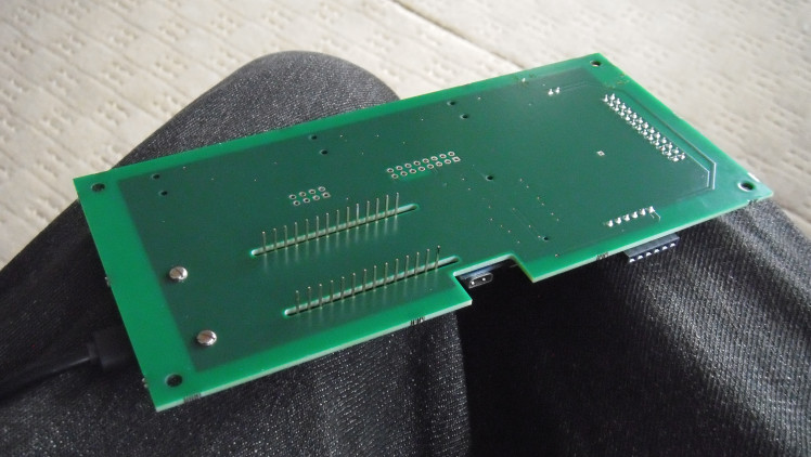
The PCB has some cut-outs: two for the long pins on the back of the Vidor 4000, so that they can poke through the board, and a side cut to allow a rather chunky micro-HDMI connector to be plugged into the Vidor for those who need video output. Some slightly odd features are the hard-wired 8-pin connectors between the PCI-E and the I2S signals for the DACs. These have thin copper tracks underneath and in the event of an error they may be cut, a header soldered in, and wire-wrapping employed to swap any wiring. Luckily the pins chosen were all correct.
Inserting the Vidor 4000...
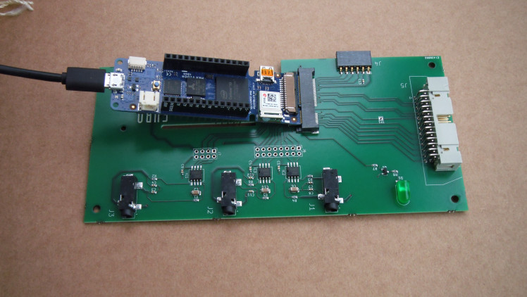
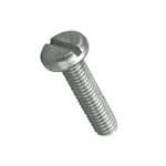
Then it's screwed down with M2 hardware:
Sustainability.
This project is not an Earth-saving scheme: for that you need solar collection plants around the planet's deserts that convert atmospheric CO2 into diesel, petrol, jet-A1 and I suppose LNG, using carbon nanotubes while reducing global warming. Three areas of 40 square km could generate enough power for the UK's grid. Not my idea, so look up Prometheus Fuels. I saw this item on SWRadiogram. But some people say that it is years behind schedule.
Shortwave Radiogram Episode 156 :: K6KZO — Captain's Log
However, my project is not a one-hit wonder. I am sure many Vidor 4000s are sitting in cupboards waiting for this extender board to arrive. It not only gives three stereo audio channels, but lets the user get at many more FPGA I/O lines above and beyond those available on the two MKR pin-headers which all seem to be shared by both FPGA and CPU. It can also be used for educational purposes.
Sound Generation.
My organ design adds up sine waves to get organ pipe sounds, though the FPGA could be used to generate sounds in a completely different manner than the simple addition of sine waves a la M. Fourier. Here are some examples.
NCOs (Numerically Controlled Oscillators), each with envelope controls, can easily be cascaded in the FPGA just like its analogue version, the Moog synthesizer. FM sound synthesis can also be done with this technique. But maybe more interesting would be to feed digital white or pink noise into Hi-Q digital filters. The filter's parameters could be varied with time. Some organ pipes produce what is called chiff for a brief period before the main hi-Q resonator gets going. This sounds a bit like a click and gives an impression of precision to the note envelope. Some experimentation is required.
Digital organs, e.g. Allen Organs, use samples, where real pipes are played and the audio captured.
An alternative use of the board: SDR.
An SSB transmitter can be built using this project and some RF upconverters. Amplified microphone input would be fed into an ADC on the CPU then the digital samples can be sent into the FPGA. The Hilbert Transform is then used to generate I and Q quadrature signals that could be mixed up to RF.
For receive, a high-speed ADC could be fed into the ribbon cable connector either as parallel signals or using high speed differential pairs.
PCBs, my history thereof.
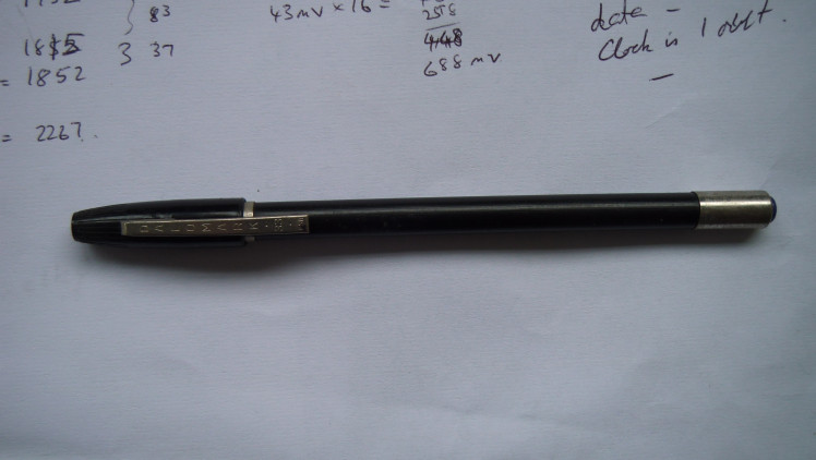
In the old days, before PCBs, tag boards were used to hold the components, and wires went from tags to valve bases as required. Allegedly the latest valve guitar amplifiers have reverted to this method of manufacture to reclaim the 'original' sound. PCBs could be made using something called a Dalo pen, which has a special black ink that would prevent copper being removed from the board by electrolysis. The board would then be drilled by hand. Here is a Dalo pen, taken from my drawer:
And here is a typical PCB made by Dalo pen (I hasten to add that it's not mine, but a 1970's organ).
Better results came from taping out a layout using thin matt black 'Brady' tape and DIL pad transfers. This was done at a 2:1 scale on transparent mylar film.
When completed, the film would be taken to be photographed and reduced to the correct size. Short bits of tape could fall off during transportation...this happened to me once.
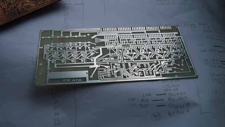
And a digital frequency meter PCB:
PCB design is so much easier these days. The only thing to be careful of is ensuring the holes are the correct diameter, because library parts are not always spot on. The software would generate Gerber files for each layer which can be e-mailed to the PCB manufacturer. The manufacturer may then look at them and count the number of holes and number of different hole diameters and come up with a quote depending on size, number of layers and material. Recently some manufacturers have an online quote system that instantly comes up with a price depending on size, quantity, turn-around time and layers. Colours and hole/via count are ignored. You don't even have to supply Gerbers for a quote.
Eurocircuits run a different scheme: just e-mail the kicad design files and it will work out a quote and point out any errors between tracks and component footprints.
My previous Electronic Organs.
My first project was started a tad over 40 years ago, and it was based on one of the published Maplin designs. It had a top-octave generator IC which gave the 12 highest notes all derived from a master oscillator. Each output was fed into a Maplin divider IC that consisted of maybe 8 flip-flops. This resulted in 96 square waves which were fed into SN74L00 NAND gates. The other input to each gate came from the keyboard.
All gate outputs were resistively combined and fed into formant band filters, selected by switches, the 'Stops'.
This did not work for a variety of reasons. The NAND gates were not perfect in the 'off' position and leaked a fair amount of signal. I think I had to add series diodes to improve that. Harmonics from the higher registers could be mixed with the fundamental square wave and produce a sawtooth wave.
Another issue was to do with the formant filters which were supposed to filter the square waves or sawtooth waves and make each rank of pipes imitate organ pipes. The filters were a mixture RC and LC tuned circuits, and would only produce the correct ratio of harmonics i.e. 'timbre', over a narrow frequency range.
Another unsatisfactory result was the fact that it was not a 'free-phase' design. All pipes of a given note e.g. middle-C played on an 8-foot pitch would produce exactly the same fundamental frequency (261Hz) whatever stops were pulled.
If one was listening to an oboe and a flute playing the same nominal note, beat notes would be heard from the very slight frequency difference and the brain would detect two different instruments playing. The design of this type of organ does not give that realism at all and you do not hear that rich effect of multiple pipes all sounding slightly off each other.
The Leslie speaker goes someway to giving a bit more realism and spring-line reverb also helps a little.
I then added an AY3-8910 3-channel programmable sound generator. These were used in arcade games and some PCs e.g. the Sinclair Spectrum. But even though it can generate white noise and perform envelope shaping, its frequency accuracy is not very good.
If you are interested in the subject, I thoroughly recommend 'Musical Application of Micro-processors' by Hal Chamberlin. It contains all you need to know on this subject including how a Numerically Controlled Oscillator (NCO) works. It has two very short programs in 6502 assembly language but otherwise is all useful information.
After a gap of many years, the next design used an Analog Devices, Inc. ADSP2101 DSP chip. I put this on a PC-AT plug-in dev board together with a 16-bit DAC. But PC technology moved on and the AT-style socket disappeared from motherboards for good before I could get this going.
Then Microchip launched a worldwide design contest in 2004 to use their dsPIC6014 dsPICDEM dev board. To one of these dev boards I added a stereo DAC and an optocoupler for MIDI input. This was now a free-phase design with each note generated by an NCO in software, and the NCO generated sine waves. DSP devices tend to have I and Q channels, so I made this organ stereo. Organ pipes are arranged so that neighbouring notes are physically separated otherwise you get sympathetic resonances. Stereo speakers can emulate pipes spread out in space and the virtual point source moves around as different notes are played. When a key is pressed, the CPU side uses look-up tables to enable multiple NCOs, one for the fundamental and one for each harmonic such that Fourier generates the correct timbre for each pipe. Obviously the LUTs have to be set up to sound like the wanted pipe e.g. flute or diapason etc. A random number generator was used to ensure that each pipe was very slightly off its nominal equal-tempered frequency.
This worked reasonably well. A single MAC opcode gave single cycle performance due to the parallel functionality inside the DSP core, though it was slowed down because of needing 32-bit wide accumulators (it's only a 16-bit processor). 60 sine waves are produced simultaneously at a sampling rate of 44kHz. The sine look-up table could be replaced by other shapes so that formant band filtering could be used. A key press could generate several sine waves at fundamental, second, third etc harmonics, each of the correct amplitude to give the stop's timbre, with independent volume for left and right channel.
Incidentally I re-purposed my two Maplin 49-note keyboards by adding a diode to each key contact and scanning groups of 8 keys with an SAB80515 8051-type CPU; it gave out MIDI serial data.
But 60 sine waves are not sufficient to simulate a pipe organ; 1,000 is more like it.
FPGA Code.
Perhaps the hardest part of writing effective FPGA code is to forget years of writing sequential code! The previous design used a DSP core, which is designed to perform lots of tasks in parallel i.e., increment data address pointers, read X and Y RAM, multiply together and accumulate in a single cycle with one opcode. That technique takes most of the thinking about concurrency away from the designer. But FPGAs take it a lot further, and the plan is to use as many 128-channel NCOs as will fit in the device. Admittedly it is possible to use the built-in, or paid for, IP, but I could only see NCOs offered with a maximum of 8 or 16 channels.
Similarly, I could have used IP for the three I2S serial digital audio outputs, but it is very easy to write a serialiser from scratch, as I have done. It worked second time; I had a slight bug that only took a few minutes to fix and retest.
At a DAC output sampling rate of 100kHz, 128 channels require a 32-bit addition at a 12.8MHz rate. If the reads, adds and writes for each channel take four steps then that leads to a clock rate of 50MHz. That is very convenient as I believe the incoming clock speed from the CPU is 48MHz.
The NCO is instantiated for each DAC channel, so that gives us 768 simultaneous sine waves. Not bad. This can easily de doubled by running another 6 NCOs in parallel and summing each pair. That assumes that there are sufficient resources in the FPGA.
How to use the FPGA.
The Arduino people have always said that they will not support 'off-piste' code for the FPGA. There are some examples of using the FPGA under the Arduino IDE to act as multiple up/down counters for rotary switches and multiple SPI ports but that is about it.
Luckily some clever people have put some templates together so that Quartus can be used to compile FPGA code which can be loaded into the FPGA by the CPU on power up. Less conveniently, but for faster boot-ups, the CPU can be programmed to act as a Byte Blaster and load the FPGA's associated flash memory with your compiled code. I use the first method, and the template was written by WG5GNR (73 and good DX!). Of particular importance to note is that this template realises that there is a 2.5V supply on I/O banks 2 and 5. Resistor stuffing allows a choice of 2.5 or 3.3V on these banks so beware!
Compiled code is fed into a small python script which does some kind of byte reversal, and a header file is duly formed. I have slightly modified it by hard-coding the input and output file names, MKRVIDOR4000.ttf and app.h respectively, so I can easily copy and paste the compiled file over into my python directory, double-click my script and after a few milliseconds, copy and paste its output, app.h, to the Arduino directory EmptySketch.
- #!/usr/bin/env python3
- # A program to reverse the bytes of a quartus generated bitstream for use
- # programming the MKR Vidor 4000 board with the Arduino IDE.
- #
- # Among the files in the output folder from quartus there is a .ttf bitstream
- # that contains comma delimited bytes represented in decimal. This program
- # flips those bytes bitwise. For example 105 (0b01101001) becomes 150
- # (0b10010110).
- # HC version: hardcoded to accept my ttf file and spit out app.h APRW
- import sys
- def reverse(num):
- binary = bin(num)
- reverse = binary[:1:-1]
- reverse += (8 - len(reverse))*'0'
- return int(reverse, 2)
- def main():
- inName = "MKRVIDOR4000.ttf"
- outName = "app.h"
- print("ReverseByteHC, Version 1.00 APRW 26th August 2022")
- print("Original version written by WD5GNR (Thanks!)")
- print("Either use ./ReverseByte.py <input file> <output file>")
- print("or ignore input files and use defaults of:")
- print(inName+" and app.h")
- if len(sys.argv) == 3:
- print('Usage: ./ReverseByte.py <input file> <output file>')
- inName = sys.argv[1]
- outName = sys.argv[2]
- print('Reversing bytes from ' + inName + ' and outputting to ' + outName)
- fpIn = open(inName, 'r')
- fpOut = open(outName, 'w')
- for line in fpIn:
- nums = [int(i.strip()) for i in line.split(',') if i != 'n']
- out = ''
- for i in nums:
- out += str(reverse(i)) + ','
- out += 'n'
- fpOut.write(out)
- fpIn.close()
- fpOut.close()
- if __name__ == '__main__':
- main()
The Arduino IDE opens EmptySketch.ino, which is not really empty but actually downloads the FPGA bitstream via a tiny JTAG loader in its Setup() subroutine/method/procedure. It is left as an exercise for the reader to modify EmptySketch for their own purposes, and I will add some kind of MIDI decoding. The CPU will then load the FPGA's dual port RAM with frequency, left and right amplitudes and DAC channel for MIDI NOTE ON messages, depending on virtual stops chosen.
I recommend learning Verilog. Most of the example FPGA code is readily available in both Verilog and VHDL languages, but SystemVerilog seems to be the new kid on the block, and I find Verilog easier to understand than VHDL. The next step is to read the 1,742 pages (approx.) of the qts_qpp_handbook. Much of this is to do with simulation, debugging and power estimation. But there are some very useful hints and tips.
One can either use the built-in IP or right-click in a source file window and add templates. The latter very useful indeed. The compiler is smart enough to recognise commonly used code and it will then use built-in resources wherever possible, such as M9K memory blocks and DSP cores.
Shift_register.v
Note that the code inclusion feature does not have verilog in its repertoire.
- `timescale 10ns/1ns
- module shift_register #(
- parameter REG_DEPTH = 32
- )(
- input clk, //clock signal, 8MHz
- input load, // load the data into shift reg
- input [REG_DEPTH-1:0] preload, // preload data
- output sdata_out, // output bit to DAC
- output lrck // LR clock to DAC
- );
- reg [REG_DEPTH-1:0] shift_reg = {REG_DEPTH{1'b0}};
- reg [REG_DEPTH-1:0] holding_data_reg = {REG_DEPTH{1'b0}} ;
- reg [4:0] ctr = 5'h0 ; // count up to 32
- always @(posedge load) begin
- holding_data_reg = preload; // load stores bus into Tx Hold Reg
- end
- always @(negedge clk ) begin
- ctr <= ctr + 1;
- if (ctr == 31) begin // so it's ready for the next clock. 220919
- shift_reg <= holding_data_reg;
- end
- else begin
- shift_reg <= {shift_reg[REG_DEPTH-2:0], 1'b0}; //load input data as LSB and shift (left) all other bits
- end
- end
- assign sdata_out = shift_reg[REG_DEPTH-1]; //MSB is an output bit
- assign lrck = ctr[4];
- endmodule
- module shift_register_tb;
- // Code your testbench here
- // or browse Examples
- parameter MSB = 32; // [Optional] Declare a parameter to represent number of bits in shift register
- reg clk; // Declare a variable to drive clock to the design
- reg ld; // load the data word into shift reg
- reg [MSB-1:0] dataword;
- wire out; // Declare a wire to capture output from the design
- wire lrck; // Declare a wire to capture output from the LRCK left/right clock
- // Instantiate design (16-bit shift register) by passing MSB and connect with TB signals
- shift_register #(MSB) U0 (
- .clk (clk),
- .load(ld),
- .preload(dataword),
- .sdata_out (out),
- .lrck (lrck));
- // Generate clock time period = 120ns, freq => 8MHz
- always #6 clk = ~clk;
- // Initialize variables to default values at time 0
- initial begin
- clk <= 0;
- ld <= 0;
- dataword <= 32'h0000f000;
- end
- // Drive main stimulus to the design to verify if this works
- initial begin
- // 1. Apply reset and deassert reset after some time
- // 2. For 10 clocks, drive alternate values to data pin
- repeat (10) @ (posedge clk)
- ld <= 1;
- #2 ld <= 0;
- // 5. Drive nothing for next 7 clocks, allow shift register to simply shift based on dir
- repeat (50) @ (posedge clk);
- // 6. Finish the simulation
- $finish;
- end
- // Monitor values of these variables and print them into the logfile for debug
- initial begin
- $monitor (" out=%b", out);
- $dumpvars;
- $dumpfile("dump.vcd");
- end
- endmodule
It's only short so I have included it here. Note two things: the first half is my 32-bit shift register, the second half is a test-bench so that the SR can be tested and debugged under ModelSim. Also note that the file only contains these two modules. To debug, shift-register.v is selected as the Top Module in Quartus, by right-clicking the filename in the Project Navigators/Files window. Please ignore all the warnings one sees about having project and top level module names identical, as that doesn't apply to using ModelSim.
Compile the code. Select Tools/Run Simulation Tool/RTL Simulation. Expand 'Work' in Library window. Double-click shift_register_tb and if there are no errors, the Objects window will come up with its internal signals. Click the signals of interest, or all, and Control+W That brings those signals into the Wave window.
Click the Run button, or type run, and the waves show up as if on a logic analyser.
Here is a trace from a real logic analyser of my three DAC I2S interfaces:
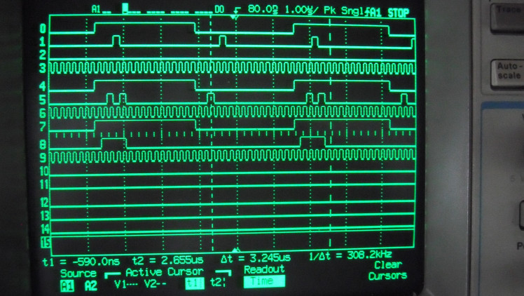
I am sending fake data to the 6 DAC channels.
The channels:
0 LRCK, DAC #1
1 SDAT, DAC #1 The first DAC has 0x1000, second has 0x2000.
2 the probe has broken so nothing to see here. Anyone got an HP 54620-61601 going free?
3 SCLK, DAC #1
4 LRCK, DAC #2
5 SDAT, DAC #2 The second DAC has 0x4000, second has 0x5000.
6 SCLK, DAC #2
7 LRCK, DAC #3
8 SDAT, DAC #3 The third DAC has 0x0000, second has 0xF000.
9 SCLK, DAC #3
DC voltages on the 3.5mm jacks are
1: 1730mV, 2: 1815mV, 3: 1980mV, 4: 2059mV, 5: 1645mV and 6: 1562mV.
They have half the gain therefore it looks as if my LRCK signal is one clock out!
But the PCB is fine/wonderful/excellent even, and it only needs a small tweak to the code to fix.
It's near the original deadline and I have yet to get my teeth into the NCOs but I am extremely pleased with progress so far.
Schematics, diagrams and documents
Code
Credits
Al
Been a keen radio amateur for many years. HF CW activity when I get the chance...homebrew radios and gadgets from valve amplifiers using EL84s etc in the past to a TV sound-bar using an Arduino and Class-D amplifier. I have been trying to build an electronic organ for a while but technology changes before I get anywhere!
Related products


Leave your feedback...