

`yaz180`

Made by feilipu / Retro Tech / Sensors / Star Wars
About the project
Modern Single Board Z180 Computer
Project info
Difficulty: Difficult
Platforms: Atmel, Seeed Studio
Estimated time: 2 days
License: MIT license (MIT)
Story
There needed to be Yet Another Z180 computer created. And so, here it is.
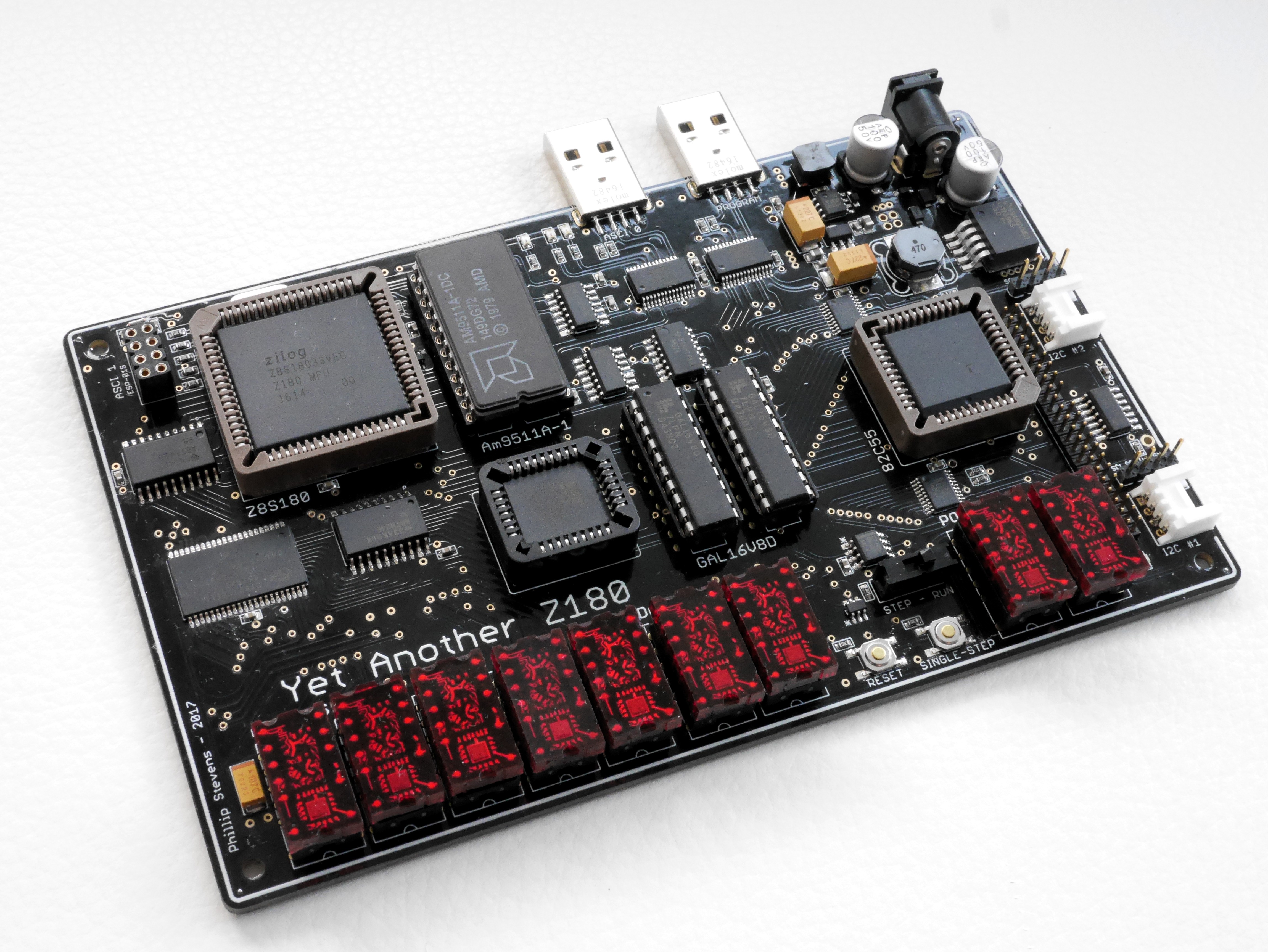
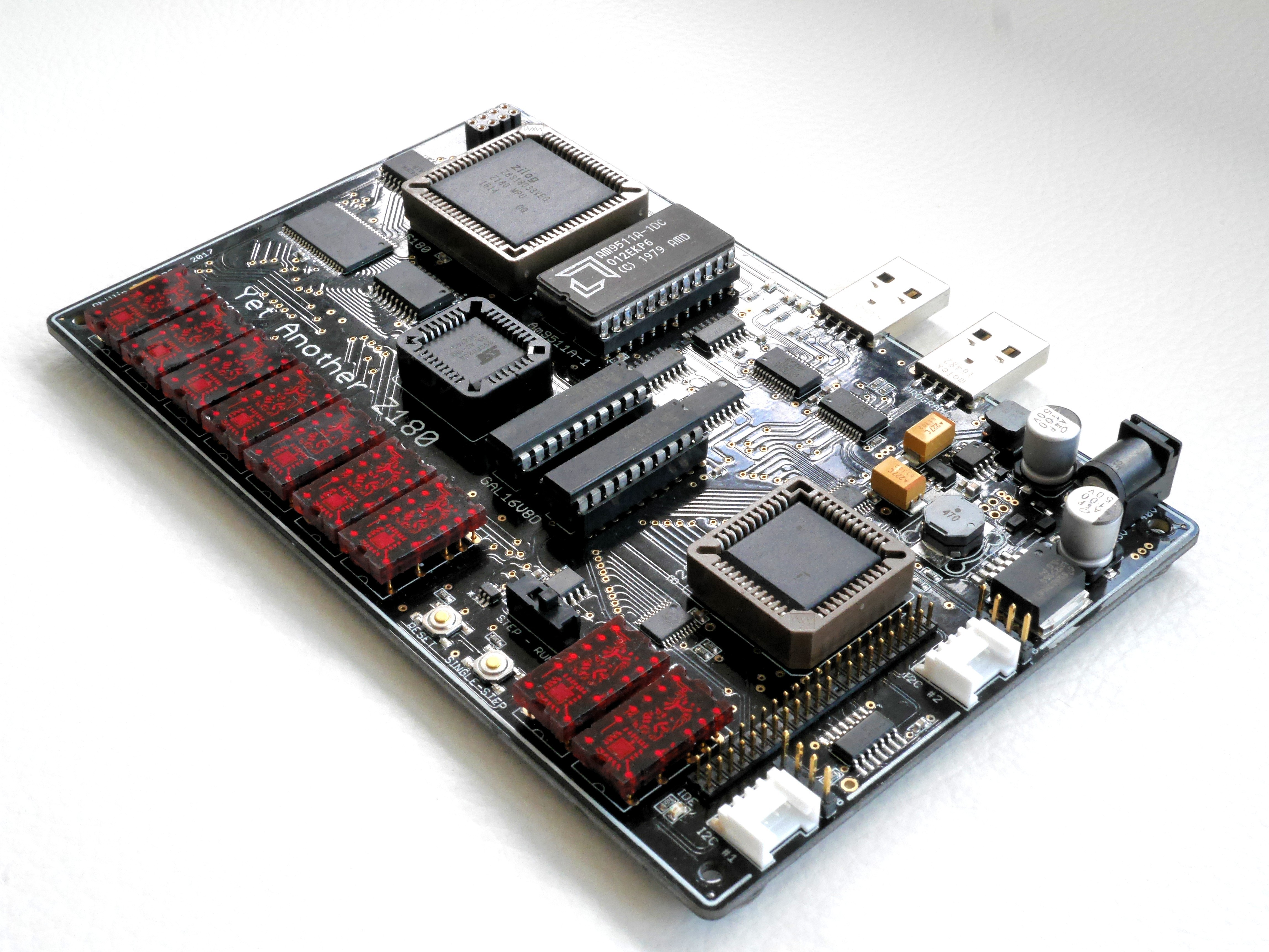
YAZ180 Version 2.1 2017 Left
 YAZ180 Version 2.1 2017 Right
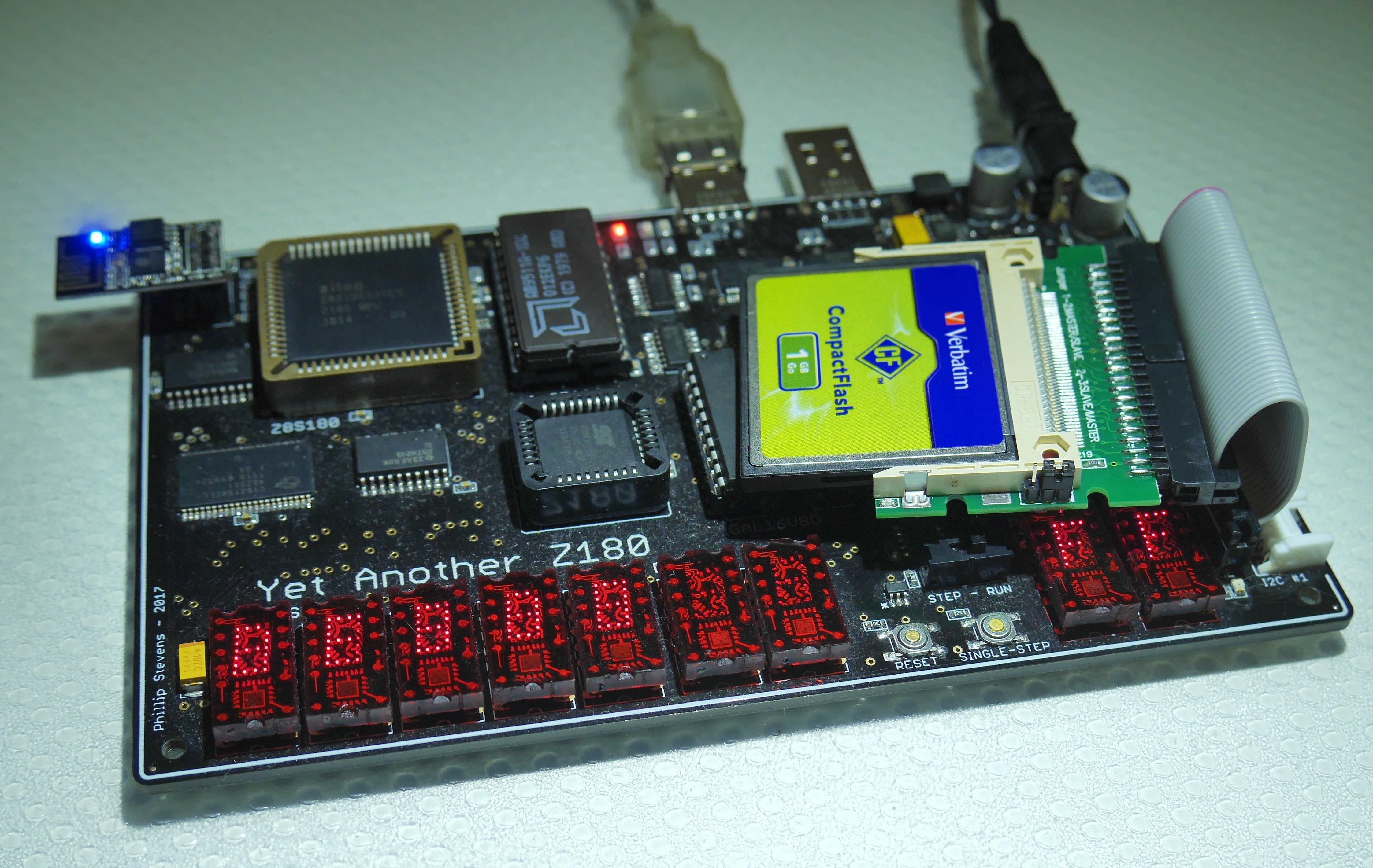 YAZ180 Version 2.1 2017 Live with yabios and CP/M
The YAZ180 is a modern single board computer, built on the tradition rich Z180 CPU and the AMD Am9511A-1 APU.
It is my attempt to create a perfect mix of "ancient" and modern computing technology. Specifically, it is an attempt to marry CPU/APU technology from 40 years ago, with modern I2C, USB, and WiFi capabilities, and make an powerful 8-bit computer that can either be embedded into an application, or operate as a stand-alone computer (with some accessories).
The YAZ180 is supported by the Z88dk and it is designed to work with both traditional CP/M v2.2 applications and modern Z88dk C compiled programs.
The YAZ180 is fully open source. All documentation and design is available from this repository. I have made the raw PCBs available on Tindie. I will find a way to get finished YAZ180 computers available shortly.
ConceptThe Z180 CPU is based on the Z80 CPU, but it includes a number of integrated peripherals including a basic Memory Management Unit (MMU), two serial interfaces (ASCI0 & ASCI1), two DMA controllers (DMAC0 & DMAC1), and two Programmable Reload Timers (PRT0 & PRT1).
The fastest readily available Flash memory is 55ns. This is matched by the fastest RAM in 8 x 1MByte packaging at 45ns. Using these two timings the fastest clock that can be therefore be supported is approximately 20MHz. Using this as a guide, and knowing that the Z180 ASCI interfaces are happiest running at a magic frequency, I have therefore selected 18.432MHz as the crystal oscillator frequency for the YAZ180.
The Z180 can operate internally at 2x the crystal oscillator frequency, which means that the YAZ180 is configured to run with PHI at 36.864MHz with 1 wait memory wait state in normal situations. This is slightly outside the Z180 specification (33MHz), but this frequency is reported to work without issues by a number of SBC builds.
The AMD Am9511A (1977) was the first hardware arithmetic Floating Point Unit (FPU) developed. It is essentially a "scientific calculator" on a chip, and is capable of both 16 bit and 32 bit fixed and 32 bit floating point processing, across all the standard and trancendental functions. Even though this device is 40 years old, it is still comparable in performance of mathematical calculations to its Z180 host.
In addition to the internal Z180 interfaces, I have added a 82C55 Programmable Peripheral Interface (PPI) Controller (1974). This device provides 3x 8 bit parallel ports, and enables the YAZ180 to support 16bit IDE hard drives, as well as providing a mechanism to add parallel data interfacing to future expansion boards.
As the IDE interface requires control signals that are active low, several of the PPI Port C lines are passed through inverters. Importantly, those Port C lines that can accept input in PPI Mode 1 or Mode 2 are not inverted, and are therefore available as inputs from off-board applications. The IDE physical interface cable also provides a tidy board extension format, to allow extension or accessory devices to be attached to the YAZ180.
A single step circuitry has been implemented, which is enabled by a switch, and triggered by writing to an I/O port address. This enables the YAZ180 to run normally, until it becomes interesting to enable a breakpoint.
To interface with modern sensors and devices, two separate I2C interface PCA9665 devices have been provided. This enables one I2C device to be running at 1MHz in Fast-mode Plus (or even Turbo mode) driving a LCD controller for a screen (for example FTDI EVE), and have the other I2C interface connected over longer distances to sensors or keyboard running at 100kHz in Standard mode. The PCA9665 has deep 68 byte hardware buffers, and can operate in buffered or streaming mode, enabling complete I2C sentences to be transmitted or received without CPU interaction. A complete GL graphics command could be sent with one CPU DMA, for example.
To interface with TCP/IP networks, using WiFi, an ESP8266 pin-out for the ESP-01S is provided, connected to ASCI1. This enables the YAZ180 to operate as an Internet server (with attached IDE hard drive), and / or to be controlled using Secure Shell from anywhere.
A USB parallel interface is provided to enable "tool-less" programming of the YAZ180. A perl script is provided to upload Intel HEX code and program it into the system Flash memory. To enable this feature hardware is provided to reconfigure the memory map to allow boot from USB.
PCBThe YAZ180 PCB is 160mm x 100mm in size, with 4 layers. This is the maximum size supported by the Eagle "Hobby Licence", which was used to create the PCB.
- Layer Top - all active devices (RED) - 2oz copper
- Layer 2 - GND layer (flood fill) - 0.5oz copper
- Layer 15 - VCC layer (flood fill) - 0.5oz copper
Layer Bottom - signal traces (BLUE) - 2oz copper
PCB Dimension - 160mm*100mm
- Material - FR-4 TG130
- Surface Finish - ENIG
- Min Solder Mask Dam - 0.4mm
- PCB Color - Black
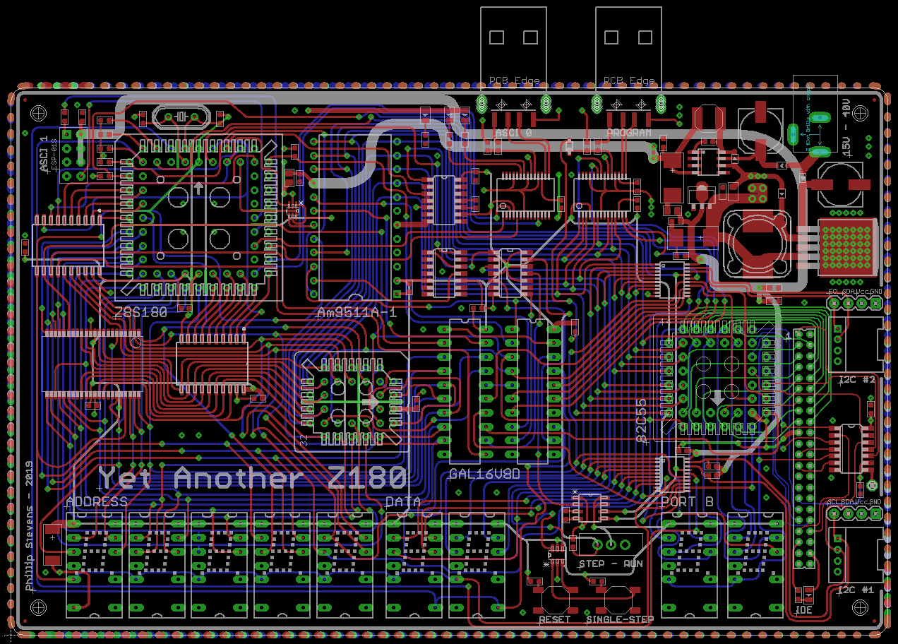
YAZ180 Version 2.4 PCB 2019 Layout
 YAZ180 Version 2.1 PCB 2017

The YAZ180 requires 15V to 40V, 2A power supply, through a standard 2.1mm barrel jack. If you are not equipping the Am9511A-1 APU, then the minimum required supply voltage drops to 7V.
The main supply is switchmode rated at 5V 3A, which is used by most of the traditional devices on the board. Note that the TIL-311 LED display devices consume approximately 105mA each, and operate HOT TO TOUCH.
A 3.3V 1A rated linear supply is fed from the 5V internal source. 3.3V is needed to support the I2C and ESP-01S devices.
The internal 12V 500mA rated switchmode supply is generated only to support the APU. Note that the Am9511A-1 consumes 5V 70mA plus 12V 70mA normally, and operates BURNING HOT TO TOUCH (seriously).
The Z180 is supported by an ABT logic signal buffer on the /RD, /WR, /MREQ, and /IORQ lines, together with the four lowest address lines, A3, A2, A1, and A0. These signals are provided to all active elements, and so even though the Z180 includes its own signal buffers, I thought these signals should be additionally buffered.
The Z180 data lines are also buffered by an ABT logic bus transceiver. This is to ensure that these lines are also optimally driven.
BOMThe Bill of Material is available from DigiKey by modifying this Shopping Cart.
Note that there are two significant items missing from the Shopping Cart.
- The Am9511A-1 is obsolete, and is only available from second tier chip sellers.
- The TIL-311 is not obsolete, but is no longer used in modern development and so is also not generally available.
Both of these products are readily available from second tier sources, but due to their scarcity they are not inexpensive.
Some other smaller pin-outs and connectors are not included:
- 2 of Seeed Studio Grove I2C connectors
The physical address mapping is provided by the standard CUPL (described below), and is completely arbitrary. Any other CUPL definitions can be programmed into the GAL16V8D "Memory" device to provide any memory layout desired.
Physical Memory Address Space
The basic layout is to allow for an initial boot from flash memory into a BANK_0, with additional BANK_1 through BANK14 containing 64kB RAM based application spaces. The upper 4kB of each application space will be masked by COMMON AREA 1 RAM, which provides system utilities.
The additional flash memory is assigned to the upper memory space (BANK13, BANK14, and) BANK15, depending on the size of flash storage equipped. This non-volatile storage can be used for any purpose.
The PROGRAMMING MODE hardware recognises that data is available on the USB parallel port, and reconfigures the physical address mapping to enable boot from USB, and further programming of Flash or RAM.
Physical Address Range Run Mode Programming Mode $00000 - $0BFFF Flash (48kB of 128kB) USB pseudo RAM (48kB) $0C000 - $DFFFF SRAM (848kB of 1MB) SRAM (848kB of 1MB) $E0000 - $EFFFF SRAM (64kB of 1MB) Flash (64kB of 128kB) $F0000 - $FFFFF Flash (64kB of 128kB) Flash (64kB of 128kB)
Logical Memory Address Space
There is no need to follow this logical address space mapping. This is what I prefer. You can do whatever you want.
The organisation below is an attempt to provide a BANK_0 containing YABIOS (CRT0, boot code, and Z88dk library code) together with a RAM system heap. The COMMON AREA 1 space from 0xF000 to 0xFFFF is intended to hold banking code, system call forwarding, interrupt service routines, system buffers, and a system stack.
Additional BANK_1 through BANK14 are intended to hold user code, whether CP/M or Z88dk C programs, both are supported through system calls to BANK_0.
Flash found in (BANK13, BANK14, and) BANK15 is intended to be used for snapshots of default or frequently used applications. For example a CP/M snapshot would enable a "diskless" CP/M initialisation, using DMA to load within fractions of a second. Suggested default snapshots could be: CP/M CCP/BDOS, CP/M + BASIC, or Webserver, for example.
Logical Address Range Run Mode Programming Mode $0000 - $BFFF Flash (48kB, BANK_0) USB (48kB, CA0) $C000 - $EFFF SRAM (12kB, BANK_0) Flash (8kB, BANK) $F000 - $FFFF SRAM (4kB, CA1) SRAM (8kB, CA1)
I/O Address Space
A computer always needs to be extended and to interact with the real world, and the YAZ180 provides multiple high-speed interfaces. As the Z180 supports 16 bit I/O addressing, the address lines A15-A13 to provide I/O selection options on the YAZ180.
Using a PLD to generate the I/O address mapping also allows flexibility to latch data into the Hex Display, or trigger breakpoints using Z180 #M1 and #Wait signals to allow Single Step execution from any code point.
I/O Address Range Chip Select (A15,A14,A13) Device $0000 - $1FFF DO NOT USE Internal I/O z180 #INTn $0000-$00FF Registers $2000 - $3FFF BREAK Break Point - Initiate Single Step Mode $4000 - $5FFF #DIO_CS 82C55 $4000-$4003 Registers $6000 - $7FFF EXPANSION Hold for Expansion $8000 - $9FFF #I2C_CS2 PCA9665 #INT2 $8000-$8003 Registers $A000 - $BFFF #I2C_CS1 PCA9665 #INT1 $A000-$A003 Registers $C000 - $DFFF #APU_CS Am9511A-1 #INT0 $C000-$C001 Registers $E000 - $FFFF EXPANSION Hold for Expansion
CUPLThe YAZ180 is essentially software defined hardware. The use of Programmable Logic Devices (PLD) to control the board has enabled me to avoid multiple rework to repair issues, and has enabled reconfiguration of memory and I/O logic without raising a soldering iron.
Memory GAL Configuration

Logic (Single Step) GAL Configuration

The YAZ180 CUPL code is available in the respective directory.
YABIOSPlease see here for status of yabios work in progress.
Currently the YAZ180 is initialised to load either yabios v1.1 or NASCOM Basic. Applications can be built the Z88dk using the ROM (raw metal), and APP (yabios) models.
The YABIOS supports CP/M 2.2 Page 0 compatibility, with an underlying Fat32 File System, and has been extended to allow access to Z88dk libraries, and APU and floating point libraries, through the use of RST+DEFW short calls, and will include a _call_far capability to allow applications to grow beyond 60kB. There is support for CP/M drives as Fat32 files on an IDE drive.
Z88dk support has been completed, and improvement work continues daily.
CP/MCP/M is complete with the console I/O, and the underlying disk sub-system working. Integration of CP/M disks as FAT32 files has also been completed. CP/M can be booted off the Flash snapshot and can load transient programs from FATFS files (read as CP/M drives).
CP/M drive files can be read and written using a host PC with any operating system, by using the cpmtools utilities, simply by inserting the IDE drive in a USB drive caddy.
There are some construction notes with errata, to advice on how to build the YAZ180.
Owners NotesThere are some owners notes advice on how to operate the YAZ180, and its environment.
Schematics, diagrams and documents
CAD, enclosures and custom parts
Code
Credits
Related products


Leave your feedback...