

Adjustable Voltage Power Supply

Made by Cris / Productivity
About the project
Adjustable voltage power supply with voltage and current control.
Project info
Difficulty: Moderate
Platforms: KiCad
Estimated time: 2 days
License: GNU General Public License, version 3 or later (GPL3+)
Items used in this project

Story
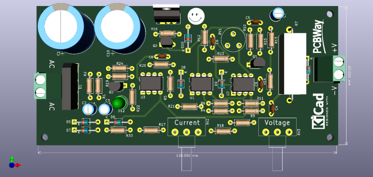
Adjustable voltage power supply
Among the most important electronic devices in the electronics laboratory is the voltage source. This source can be linear, switching mode, adjustable or not, but it is very useful for powering various electronic assemblies.
The circuit below proposes a linear voltage source, adjustable, of medium power, being able to support loads up to 70W-80W in some cases.
Functionality
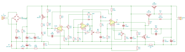
This circuit is supplied from the primary side of a transformer with a secondary winding calculated to discharge 24 VAC at 3 A. The alternating voltage is rectified by the diode bridge B1 and then filtered with the filter composed of the capacitor C1 and the resistor R1.
The schematic includes some original elements that make it quite different from other power supplies in its class. Instead of using a feedback loop to control the output voltage, this circuit uses a constant gain amplifier to obtain the reference voltage required for stable operation. The reference voltage is generated at the output of operational U1. The current passing through R8, the 5.6V Zener diode D8, R5 and R6 makes us obtain a very interesting voltage reference. The voltage of 5.6V appears on R5. Through R6, which has the same value as R5, passes the same current (the current at the input of the operational is negligible) so that the voltage collected from R5 and R6 at the output of the operational U1 will be 11.2V, ie twice the value of the reference voltage of the diode Zener.
The next floor is an amplifier made with the U3 circuit that has a constant amplification of about 3 times, established with the relation A = (R11 + R12) / R11. This floor raises the reference voltage from 11.2V to 33V. Voltage limits are set with RV3 and R10. With R10 the offset is adjusted and the minimum voltage is set to 0V and with RV3 the voltage in the range 0-30V is varied.
Another original element is the constant current generator converted from a constant voltage source. The voltage read from R7, the shunt current resistance, from which the load current is measured, is applied to the non-inverting input of the circuit U3 and the inverting input reads the output current to ground (potential 0V) through the resistance R21. The regulated potential from RV2 is also applied on the non-inverting input, potential set by the values ??of the components at minimum 1V. As the load current increases, the voltage will remain constant thanks to the error amplifier U2. If the voltage on R7 increases above 1V, the circuit U3 switches to the constant current generator mode and through the diode D9 connected to the non-inverting input of U2 which controls the output voltage through the series regulator. This type of connection allows the accuracy of maintaining the output current at constant levels of up to 2mA.
The capacitor C8 has the role of stabilizing the circuit at sudden variations. By exiting the operational U3, together with the control of U2 when the voltage decreases (increasing the current per load) the transistor Q3 will also be controlled, which, through the collector current, allows the LED to signal the exceeding of the regulated limit current in RV2. A negative voltage doubler scheme with C2, C3, D5 and D6 is used, using the pulsating voltage on the rectifier bridge, thus obtaining a negative voltage which is then limited by R3 of the Zener diode D7. This creates the negative voltage line that supplies U2, U3 and through R14 the command to block through Q1 the output voltage when the negative voltage drops (Q1 would enter the conduction, Q2, Q3 blocked). This method is a great advantage in the case of a shortcircuit, experimental laboratory test. In the vast majority of stabilizer schemes, when a voltage drops, the charged filter capacitors can still generate currents through the open regulators which can thus cause significant damage to the circuit.
Calibrating the circuit
- Potentiometers RV3 and RV2 are brought to a minimum;
- Measure the voltage after rectification, on the filter capacitors (32-34V);
- Check the negative voltage on the Zener diode D7 (5.6V);
- Connect the voltmeter to the output on the 200V range;
- Adjust the semi-adjustable RV1 to obtain the voltage of 0V at the output;
- Connect a resistive load to the output (16-30Ω). The load can be a 30-60W resistor immersed in a container with water for cooling;
Check the voltage setting in RV3 and the current limiting setting in RV2. By turning counterclockwise, the LED will light up and the current will go into limitation.
Leave your feedback...