
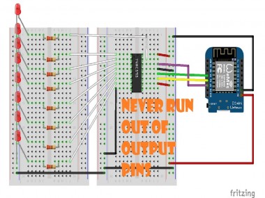
Never Run Out of Output Pins
Made by talofer99
About the project
HC595 shift register to the rescue!
Project info
Difficulty: Easy
Estimated time: 1 hour
License: GNU Lesser General Public License version 3 or later (LGPL3+)
Items used in this project
Hardware components


Story
Like most of us, I ran out of output pins once or twice over the years. At times I just went with a bigger board, like moving from Uno to Mega. But at times it just didn’t make any sense. so to solve this, let me introduce you today to the great 8bit shift register –that allow us with the small price of 3 GPIOS to gain at least 8 outputs, and you can daisy-chain many more.
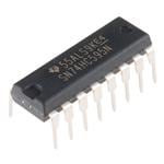
For this tutorial I choose a hc595 shift register, there are many different makers and modules, they vary in their electric specs, mainly current rate. But they all work the same way, when it comes to the code and the wiring. one of the coolest feature of this chip is that you can daisy-chain more than one to it. Let’s start by covering the chip pin out and the wiring needed to start working with it. will use the great written tutorial on the Arduino web site as a reference. ttps://www.arduino.cc/en/tutorial/ShiftOut
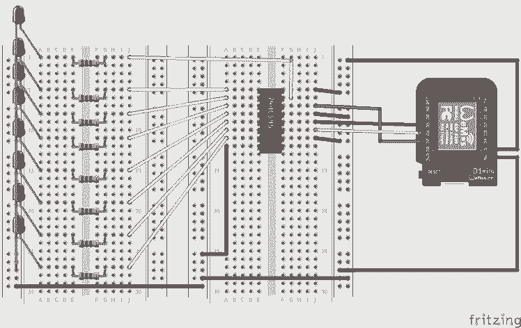
I did not see any example of hooking it up to a esp8266 so I decided to use one for this tutorial.
on the left we got Q1 -> Q7 and the second top right the Q0, thus are the output pins. The next important pins are the clock pin, the latch click pin and the serial data input.
I will mention MR and OE, thus are left out in this example, and the only down side of it is that the lights will turn on to their last state or something arbitrary every time you first power up the circuit before the program starts to run.
hooking it up is simple, and we got a great diagram and image for this in the tutorial.
SERIAL DATA INPUT (DS pin 14) to wemos D7 (blue wire)
CLOCK PIN (SH_CP pin 11) to weos D6 (yellow wire)
CLOCK PIN LATCH (ST_CP pin 12) to wemos D5 (green wire)
Note that the LED have resistors, the original post talks about 470Ohm I used 220Ohm and I think it’s more than enough. At times, if the LED flicker you will need to add a 0.1"f capacitor between the latch pin and ground.
After all this hard work of wiring lets skip into the code and see how this magic works.
//Pin connected to ST_CP of 74HC595
int latchPin = D5; //8;
//Pin connected to SH_CP of 74HC595
int clockPin = D6; //12;
////Pin connected to DS of 74HC595
int dataPin = D7; //11;
void setup() {
 //set pins to output so you can control the shift register
 pinMode(latchPin, OUTPUT);
 pinMode(clockPin, OUTPUT);
 pinMode(dataPin, OUTPUT);
}
We define global variable for each of the pins, so it will easy to refer to them later in the code. in the setup we set all of them as OUTPUT pins.
void loop() {
 // count from 0 to 255 and display the number
 // on the LEDs
 for (int numberToDisplay = 0; numberToDisplay < 256; numberToDisplay++) {
   // take the latchPin low so
   // the LEDs don't change while you're sending in bits:
   digitalWrite(latchPin, LOW);
   // shift out the bits:
   shiftOut(dataPin, clockPin, MSBFIRST, numberToDisplay);
   //take the latch pin high so the LEDs will light up:
   digitalWrite(latchPin, HIGH);
   // pause before next value:
   delay(500);
 }
}
This code counts from 0 (zero) to 255, and send this number to the chip. In order for the chip to know he is about to get data,
we set the latch pin to low,
we do the shift of data using the shift out command
and we set the latch pin back to high to signal the chip we are done and to output it on the Q0->Q7
The value that is passed, will be represented in binary on the LED. If you never done any binary math before, I got a video on this as well
Very important parameter in the shiftout function that I did not cover before is the bit order. It got 2 options MSBFIRST or LSBFIRS. Which refer to which will be the first bit to be pushed into the chip – the less or more significant one, and the end result will be how its displayed on q0 to q7. If we take the previous example, and change the bit order will get the reversed result in the LED
Now adding 8 output pins in the price of 3 GPIO its ok but not amazing. But as I mention in the beginning, we can daisy chain them. So now let’s look into how we do that. We will extend the clock and latch pins to the 2nd chip,
and we will connect the Serial OUTPUT pin (pin9) of the first chip to the Serial INPUT pin (pin 14) of the 2nd one.
Connect all the needed power wires, resistors and LED. and we are ready to go. With the current code we can see that its working, and the 2ndIC is -1 from the first IC value. Due to the fact that we shift one value at a time, and once we do so, the previous one gets shifted from the first IC to the second one This code, that changes both IC to the same value by doing 2 shift out between each latching.
Schematics, diagrams and documents
Code
Credits
Related products


Leave your feedback...