
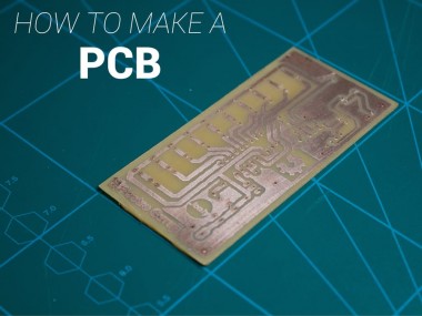
DIY PCB Etching

Made by ElectroGuruji
About the project
Learn how to make a printed circuit board at home using the iron & laser printer method and ferric chloride etchant.
Project info
Items used in this project

Story
Learn How to Make a Printed Circuit Board at home using the Iron & Laser Printer method and Ferric Chloride Etchant.
Don't forget to Subscribe for more projects: YouTube
Step 1: Parts & Materials
- Copper Clad PCB - AliExpress
- Ferric Chloride Etching Solution
- PCB Drill + Bits - AliExpress
- Sandpaper
- Paper Cutter
- Permanent Marker
- Laser Printer
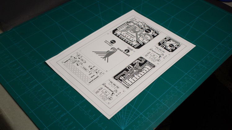
Step 2: Export Settings
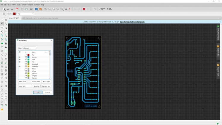
Once you have finished designing the board layout of your circuit in Eagle, go to Layer Settings and select Hide Layers.
Next, select only the following layers for a bottom layer only PCB:
- 16 - Bottom
- 17 - Pads
- 18 - Vias
- 20 - Dimension
- 45 - Holes
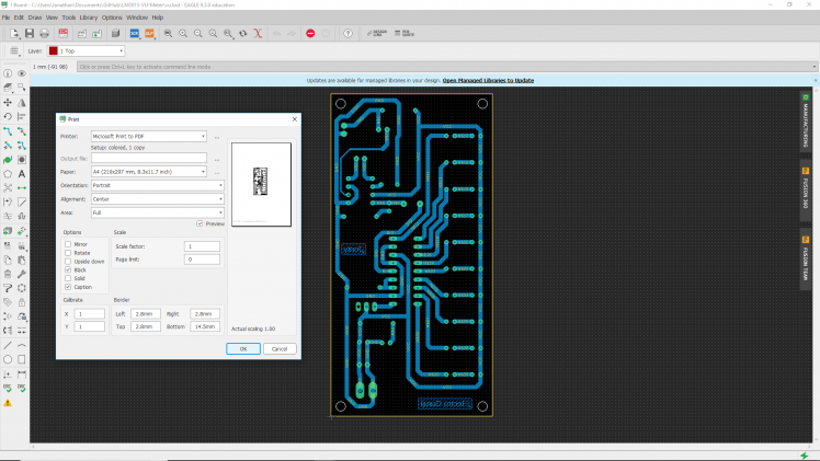
Then go to File>Print. Set the Printer to Microsoft Print to PDF.
Ensure that the following settings are also selected: Black and Caption.
Click OK and Save the file in the destination folder of your choice.
Step 3: Printer Settings

Print out the PDF file using a Laser Cutter on a sheet of Glossy Photo paper.
Ensure that the print scale is 1.0
Do not change any other printer settings.
Step 4: Cut the Image
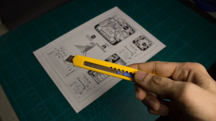

 Cut the PCB image to size using a paper cutter and scale.
Step 5: Cut the PCB
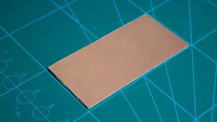
Mark the dimensions of the image on to the PCB using a permanent marker. Then use a paper cutter and scale to cut the PCB to the correct size.
Step 6: Iron the PCB
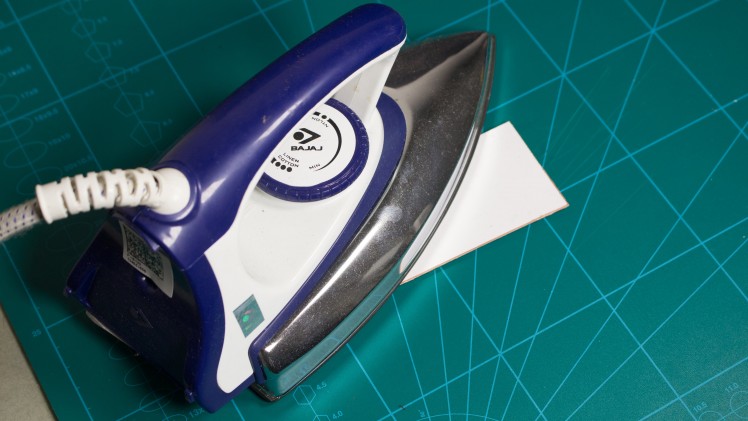
 Sand the PCB using a fine grit of sandpaper and some water.
Place the image directly upon the copper side of the PCB and iron it for approximately 10 minutes.
By doing so the laser printed ink will get transferred from the photo paper to the surface of the PCB.
Remove the excess paper with some water so that you are only left with the stained PCB.
Step 7: Etch the PCB
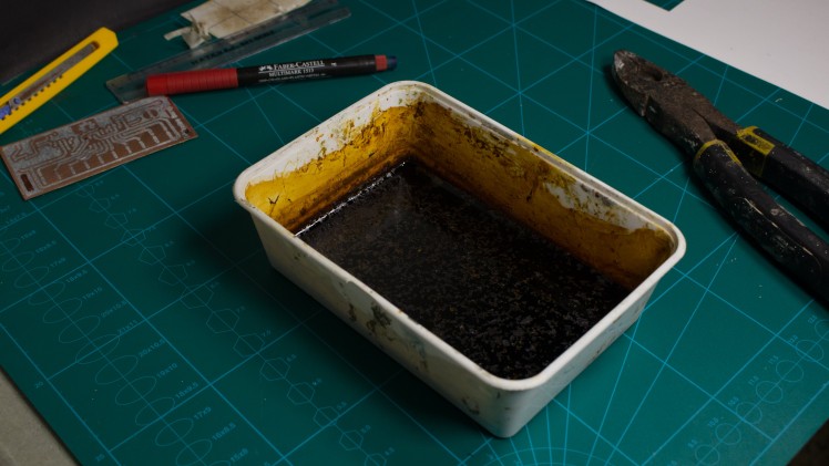
I made a solution of Ferric Chloride and Water. When we mix these two, an exothermal reaction takes place and hence we must mix the solution preferably in a plastic or glass container. Do not mix the solution in a metal container.
Shake the container for approximately 10 minutes. The acidic solution will slowly etch the unexposed copper. You can speed up the process by adding more ferric chloride.
Step 8: Drill Holes
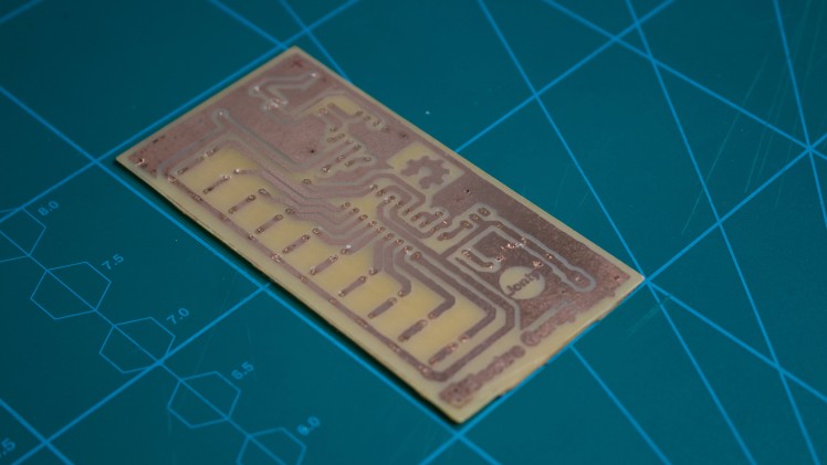
I used an electric drill to drill holes for the components. You can also use a manual PCB drill to do so.
I also used a larger sized drill bit to drill holes for the mounting standoffs.
Step 9: Support These Projects
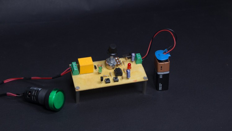
Some of the circuits I have made using this PCB fabrication method.
YouTube: Electro Guruji
Instagram: @electroguruji
Hackster: ElectroGuruji
Facebook: Electro Guruji
Schematics, diagrams and documents
Code
Credits
Related products


Leave your feedback...