
5v And 3.3v Level Signal Conversion Problems And Methods

Made by Alanlin
About the project
Talking about problems and methods 5V and 3.3V level signal conversion
Project info
Difficulty: Easy
Platforms: AllThingsTalk, C.H.I.P, circuito.io
Estimated time: 1 hour
License: GNU General Public License, version 3 or later (GPL3+)
Items used in this project

Story
Now there are more and more low-voltage and low-power devices, and 3.3V and 2.1V level signals are becoming more and more common. This presents a level shifting problem. Of course, conversion is not needed in many cases, and some devices are more inclusive. Whether it can accommodate multiple levels needs to check the IC manual. If the different voltages can be tolerated, the AC conversion unit is not needed.
In addition, the conversion circuit will definitely limit the communication speed and stability. There are two things to keep in mind before converting.
1. ABSOLUTE MAXIMUM RATINGS
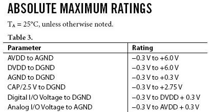
This is a limit parameter to ensure the safety and health of the IC. Do not exceed this range when applying the connection. For example: DVDD (analog power supply) to DGND (analog ground) voltage range is -0.3V to +6.0V; digital I/O port voltage to ground voltage range is -0.3V to +vdd+0.3V.
2. Whether the level signal conversion unit is needed or not, see the following parameters:
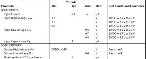
It can be seen that the low-level threshold of this IC's digital logic input is <0.7V (3.3V case); the high-level threshold is >2V (3.3V case); of course, these parameters are limited to ABSOLUTE MAXIMUM RATINGS.
To sum up, it is the "five elements" of level conversion:
( 1) Level compatible
To solve the problem of level conversion, the most fundamental thing is to solve the level compatibility problem of the logic device interface. There are two principles of level compatibility: VOH > VIH; VOL < VIL.
Of course, considering the anti-interference ability, there must also be a certain noise tolerance:
|VOH-VIH| > VN+; |VOL-VIL| > VN-.
where VN+ and VN- represent positive and negative noise margins.
As long as you master this principle and are familiar with the input and output characteristics of various devices, you can naturally find a reasonable solution.
( 2) Power sequence
Issues that must be paid attention to in multi-power systems. Some devices do not allow the input level to exceed the power supply, and if the input is added without the power supply, it is likely to damage the chip. The best way to perform in this situation is probably to use 164245. If the speed allows, the method of using a transistor or a current limiting resistor can also be considered.
( 3) Speed/Frequency
Some conversion methods affect the working speed, so attention must be paid. Like some schemes, due to the existence of resistance, charging the load capacitance through the resistance will inevitably affect the speed of the signal edge. In order to increase the speed, the resistance must be reduced, which in turn increases the power consumption.
( 4) Output drive capability
This one is actually the same as the previous one, because the key to the speed problem is the ability to charge the load capacitor.
( 5) Number of channels
Some solutions have more components, or the wiring is inconvenient, and the number of channels becomes a problem.
( 6) Cost & Supply
The 164245 mentioned earlier has this problem. The "Five Elements" pops up as a 6th because it's a non-technical factor and it's so fundamental that it can be ignored.
Let's take a look at the level conversion method.
1. Lower level to higher level (such as 3.3V to 5V):
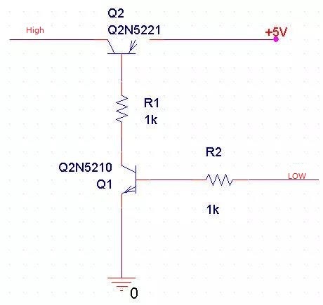
"Low" is connected to a lower level signal; "High" is connected to a higher level signal.
Two transistors ensure the same polarity of the signals at both ends.
2. From higher level to lower level (such as 3.3V to 5V):
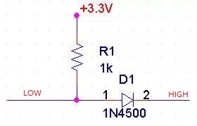
Analysis: When the "high" (+5V level signal) output is logic 1, the diode is turned off (equivalent to disconnection), and the low is pulled up to about +3.3V. When the output at "low" (+5V level signal) is logic 0, the diode is turned on. Ideally, the voltage at "low" is turned on to 0. The actual voltage at "low" is the diode conduction voltage drop (about 0.7V, If you think it is high, you can use a Schottky diode, and the Schottky diode has a small voltage drop).
There are some level signal conversions that can use comparators. I have seen this application in a comparator manual before. It is also very convenient, but the cost is a bit high. I heard some netizens say that a small resistor can be connected between signals of different levels to solve the problem. I also tried this (3.3V cyclon2 communicates with 5V MCU), it seems to work normally, but it always feels not very stable.
To sum up, the common methods of level conversion are:
( 1) Transistor + pull-up resistor method
It is a bipolar transistor or MOSFET. The C/D pole is connected to a pull-up resistor to the positive power supply. The input level is very flexible, and the output level is roughly the positive power supply level.
( 2) OC/OD device + pull-up resistor method
Similar to 1). Suitable for occasions where the device output is just OC/OD.
( 3) 74xHCT series chip boost (3.3V→5V)
Any 5V CMOS device whose input is compatible with the 5V TTL level can be used as a 3.3V→5V level shifter. ——This is because the level of 3.3V CMOS is just compatible with the level of 5V TTL (coincidence), and the output level of CMOS is always close to the power level.
Inexpensive options such as the 74xHCT (HCT/AHCT/VHCT/AHCT1G/VHCT1G/...) series (that letter T means TTL compatible).
( 4) Over-limit input step-down method (5V→3.3V, 3.3V→1.8V, ...)
Any logic device that allows the input level to exceed the power supply can be used to reduce the level. "Overrun" here means exceeding the power supply, and many older devices did not allow input voltages to exceed the power supply, but more and more new devices remove this limit (change the input stage protection circuitry).
For example, the datasheets of the 74AHC/VHC series chips clearly indicate that "the input voltage range is 0~5.5V", and if a 3.3V power supply is used, 5V→3.3V level conversion can be achieved.
( 5) Dedicated level conversion chip
The most famous is the 164245, which can not only be used as a boost/buck, but also allows the two sides of the power supply to be out of sync. This is the most common level-shifting scheme, but it is also expensive, so the first two schemes are best used unless necessary.
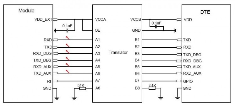
For example, the serial port voltage domain of the BC26 module of Shanghai Quectel is 1.8V. If the voltage domain of the customer application system is 3.3V, a level converter needs to be added to the serial port connection between the module and the customer application system. Texas Instruments' TXS0108EPWR is recommended. The reference circuit is as follows:
( 6) Resistance divider method
The easiest way to lower the level. 5V level, divided by 1.6K+3.3K resistor, is 3.3V.
( 7) Current limiting resistance method
If the above two resistors are too many, sometimes only one current limiting resistor can be connected in series. Although some chips do not allow the input level to exceed the power supply in principle, as long as a current limiting resistor is connected in series to ensure that the input protection current does not exceed the limit (for example, 74HC series is 20mA), it is still safe.
Leave your feedback...